Semiconductor memory device control method and semiconductor memory device

a memory device and semiconductor technology, applied in the direction of information storage, static storage, digital storage, etc., can solve the problems of insufficient reduction of average current consumption for overall dram, consumption of a current from an external power supply, and inability to reduce average current consumption more. to achieve the effect of reducing average current consumption

Active Publication Date: 2006-01-24
LONGITUDE LICENSING LTD
View PDF9 Cites 77 Cited by
  • Summary
  • Abstract
  • Description
  • Claims
  • Application Information

AI Technical Summary

Benefits of technology

[0011]It is therefore an object of the present invention to provide a semiconductor memory device control

Problems solved by technology

However, even if the performance of memory cells and the like is improved to extend maximal data hold time tREFmax, the average current consumption cannot be reduced more after maximal data hold time tREFmax has reached a certain length.
This is attributed to a current consumed by peripheral circuits, and the existence of a DC current component such as a leak current which flows into defective sites that were unintentionally fabricated in DRAM during the manufacturing.
Thus, the highly miniaturized memory array unit suffers from a larger number of

Method used


Image

  • Semiconductor memory device control method and semiconductor memory device
  • Semiconductor memory device control method and semiconductor memory device
  • Semiconductor memory device control method and semiconductor memory device

Examples


first embodiment

(First Embodiment)

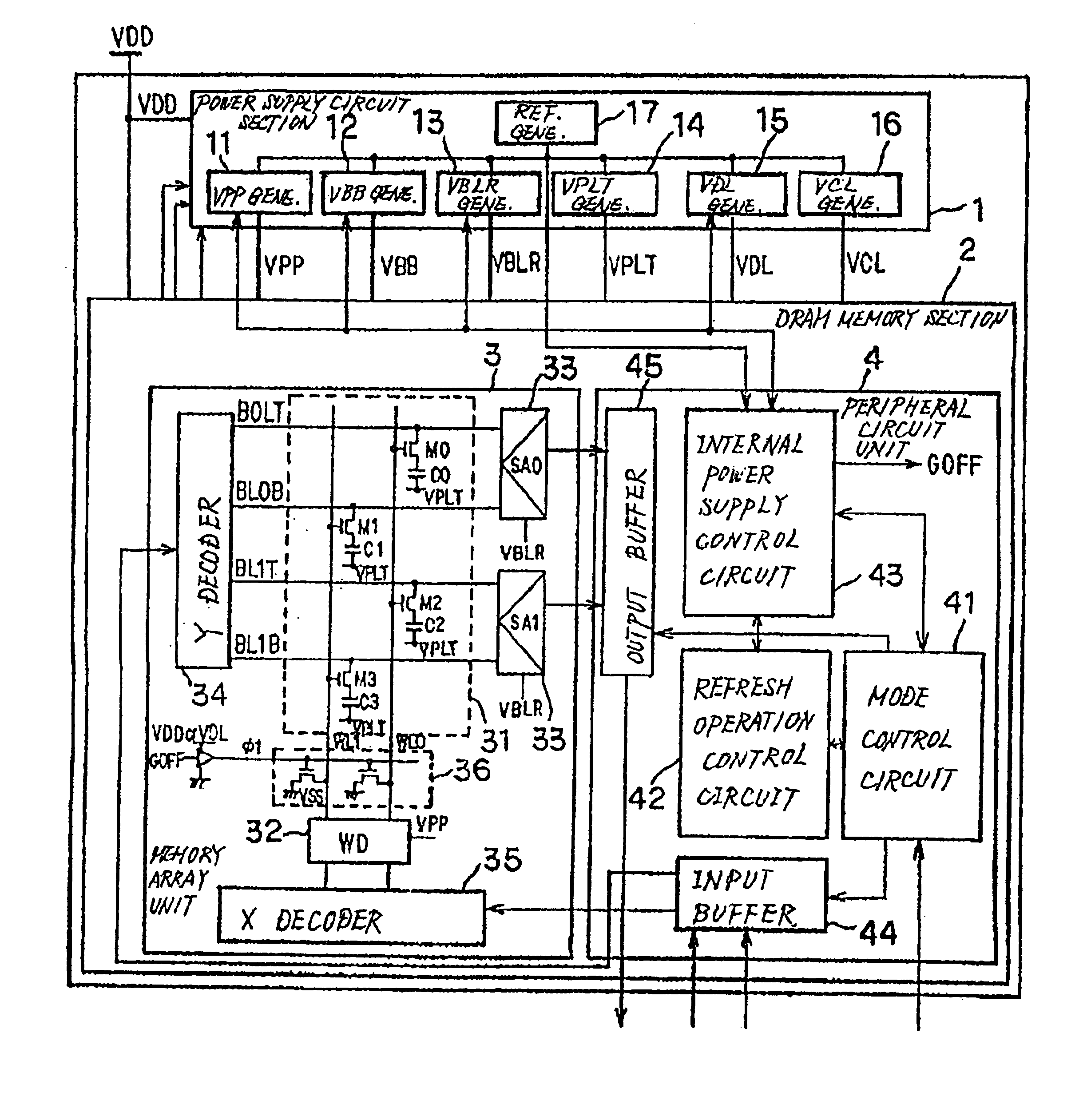
[0036]FIG. 1 illustrates the configuration of a semiconductor memory device according to the present invention in a first embodiment. Specifically, FIG. 1 illustrates an exemplary configuration of DRAM.

[0037]As illustrated in FIG. 1, the semiconductor memory device in the first embodiment comprises power supply circuit section 1 including internal voltage generator circuits respectively for generating predetermined internal supply voltages; and DRAM memory section 2 including a memory array unit for holding data and a control circuit therefor.

[0038]Power supply circuit section 1 comprises VPP internal voltage generator circuit 11 (VPP GENE.) for generating word line voltage VPP; VBB internal voltage generator circuit 12 (VBB GENE.) for generating memory array substrate voltage VBB; VBLR internal voltage generator circuit 13 (VBLR GENE.) for generating bit line precharge voltage VBLR; VPLT internal voltage generator circuit 14 (VPLT GENE.) for generating cell plate ...

second embodiment

(Second Embodiment)

[0084]FIG. 13 illustrates the configuration of the semiconductor memory device according to the present invention in a second embodiment.

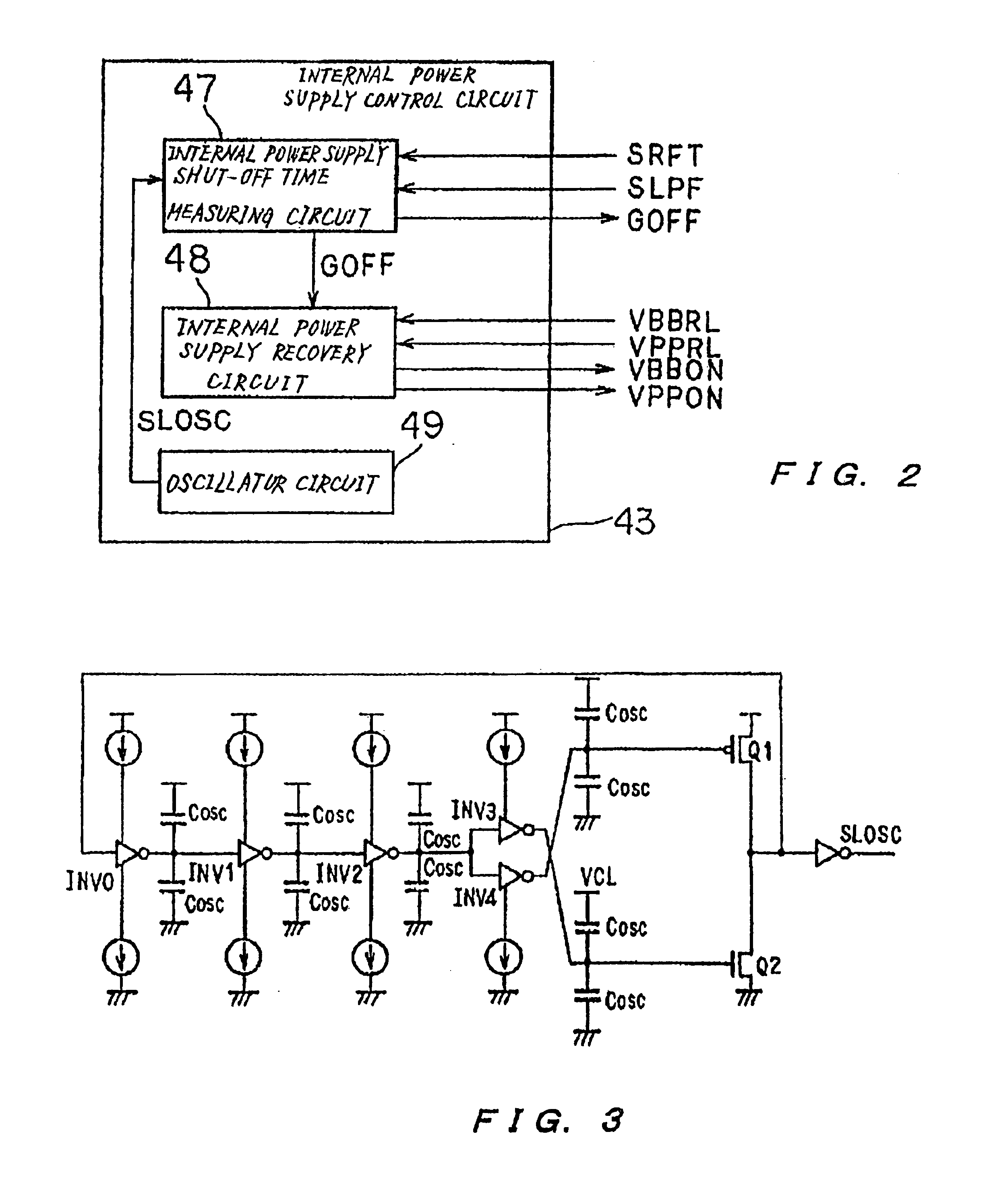
[0085]In the second embodiment, the operation of VPP internal voltage generator circuit 11 for generating word line voltage VPP is not stopped in response to internal power supply stop signal GOFF delivered from internal power supply control circuit 43. In addition, in the second embodiment, each of pMOS transistors contained in logical circuits and the like within the word driver and X decoder, which are supplied with word line voltage VPP, is supplied with word line voltage independently at its source and substrate, as illustrated in FIG. 13. Further, switching transistor Q100 is disposed between the output terminal of VPP internal voltage generator circuit 11 and the source of the pMOS transistor for disconnection therebetween. The remaining configuration of the semiconductor memory device in the second embodiment is similar t...


PUM


Abstract

In a semiconductor memory device which requires a refresh operation, a control method stops supplying a word line voltage which is a boosted voltage higher than an external supply voltage, a memory array substrate voltage which is a negative voltage supplied to a semiconductor substrate, and a bit line precharge voltage for use in reproducing data held in memory cells for a predetermined period at the end of each refresh operation. In this event, voltage output terminals of the word line and memory array substrate voltages are respectively driven to a ground potential. For recovering these voltages, the delivery of the word line voltage is stopped until the memory array substrate voltage rises to some extent.

Description

BACKGROUND OF THE INVENTION[0001]1. Field of the Invention[0002]The present invention relates to a semiconductor memory device control method suitable for application in DRAM (Dynamic Random Access Memory) which requires a refresh operation, and a semiconductor memory device.[0003]2. Description of the Related Art[0004]Recent semiconductor memory devices such as DRAM are used as well in mobile terminal devices such as portable telephones, PDA (Personal Digital Assistance), and the like, so that a reduction in current consumption is increasingly required for the semiconductor memory devices.[0005]As a means for realizing a reduction in current consumption, Japanese Patent Application Laid-open No. 8-203268, for example, discloses a technique which places bit lines in a floating state in a non-access period for memory cells which hold data to eliminate leak currents flowing through bit lines and sense amplifiers connected thereto, thereby reducing the current consumption. The non-acce...

Claims


Application Information

Patent Timeline
IPC IPC(8): G11C7/00G11C11/401G11C11/407G11C11/403G11C11/406G11C11/4074
CPCG11C11/4074G11C11/406G11C11/401
Inventor HASHIMOTO, TAKESHIITO, YUTAKA
Owner LONGITUDE LICENSING LTD
Why Eureka
Try Eureka