Gallium nitride-based light emitting device having ESD protection capacity and method for manufacturing the same

a protection capacity technology, which is applied in the direction of semiconductor devices, roads, constructions, etc., can solve the problems of light emitting devices are more vulnerable to electrostatic discharge, and gallium nitride-based light emitting devices are more vulnerable to reverse esd than forward esd, so as to enhance the tolerance of reverse esd and enhance the reliability of the devi

Inactive Publication Date: 2006-07-20
SAMSUNG ELECTRONICS CO LTD
View PDF5 Cites 63 Cited by
  • Summary
  • Abstract
  • Description
  • Claims
  • Application Information

AI Technical Summary

Benefits of technology

[0013] When a reverse ESD voltage is applied to the light emitting device, the MIM type tunnel junctions allow tunneling of electrons therethrough. Thus, the light emitting device of the invention is prevented from being damaged by the reverse ESD voltage.
[0025] The present invention provides the gallium nitride-based light emitting device having high tolerance to reverse ESD. In order to enhance tolerance to reverse ESD, the two or more MIM type tunnel junctions are formed at locations spaced from the n-side electrode on the n-type GaN-based clad layer. Each of the MIM type tunnel junctions has a multilayer structure of metal-insulator-metal, and allows reverse current to pass therethrough when a reverse ESD voltage is applied to the gallium nitride-based light emitting device. As a result, even though the reverse ESD voltage is applied thereto, the light emitting device is prevented from being damaged, thereby enhancing reliability of the device.
[0026] Additionally, according to the invention, the material for the n-side electrode, transparent electrode layer, the p-side electrode and passivation film of the light emitting device can be used as the material for the lower metal layers, the upper layer and the insulating film constituting the MIM type tunnel junctions without using other materials, thereby reducing the manufacturing costs. The light emitting device of the invention is a compound semiconductor light emitting device, and is formed of a GaN-based material. Here, the term “GaN-based material” means a material having the formula AlxGayInzN (0≦x≦1, 0≦y≦1, 0≦z≦1).

Problems solved by technology

Although the gallium nitride-based light emitting device has a significantly large energy band gap, it is vulnerable to electrostatic discharge due to its negative crystallinity.
In particular, as the amount of crystal defects is increased, the light emitting device is more vulnerable to the electrostatic discharge.
As such, the gallium nitride-based light emitting device is more vulnerable to the reverse ESD rather than the forward ESD.
Thus, when a large reverse ESD voltage is applied in a pulse shape to the gallium nitride-based light emitting device, the light emitting device is deteriorated or damaged.
As a result, such a reverse ESD phenomenon damages reliability of the gallium nitride-based light emitting device as well as causing a sharp reduction in life span thereof.
However, with this method, there is a limitation in achieving desired tolerance to ESD.
However, in this method, an additional Zener diode must be purchased, and then assembled thereto by bonding, thereby significantly increasing material costs and manufacturing costs as well as restricting miniaturization of the device.
However, the method of protecting the light emitting device from ESD using the Schottky diode has a drawback of complicated manufacturing process.
In particular, there are problems of limitation in selection of the metallic material forming Schottky contact between the n-type GaN-based materials, and of possibility of change in contact properties of semiconductor-metal in following processes, such as heat treatment.

Method used


Image

  • Gallium nitride-based light emitting device having ESD protection capacity and method for manufacturing the same
  • Gallium nitride-based light emitting device having ESD protection capacity and method for manufacturing the same
  • Gallium nitride-based light emitting device having ESD protection capacity and method for manufacturing the same

Examples


Embodiment Construction

[0036] Preferred embodiments will now be described in detail with reference to the accompanying drawings. It should be noted that the embodiments of the invention can be modified in various shapes, and that the present invention is not limited to the embodiments described herein. The embodiments of the invention are described so as to enable those having an ordinary knowledge in the art to have a perfect understanding of the invention. Accordingly, shape and size of components of the invention are enlarged in the drawings for clear description of the invention. Like components are indicated by the same reference numerals throughout the drawings.

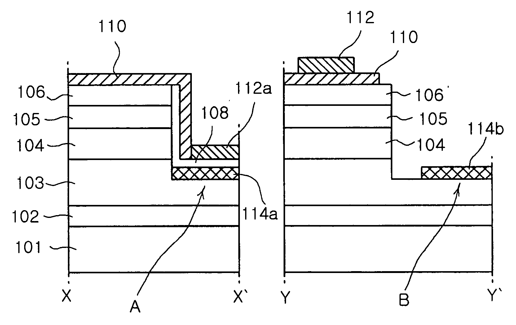
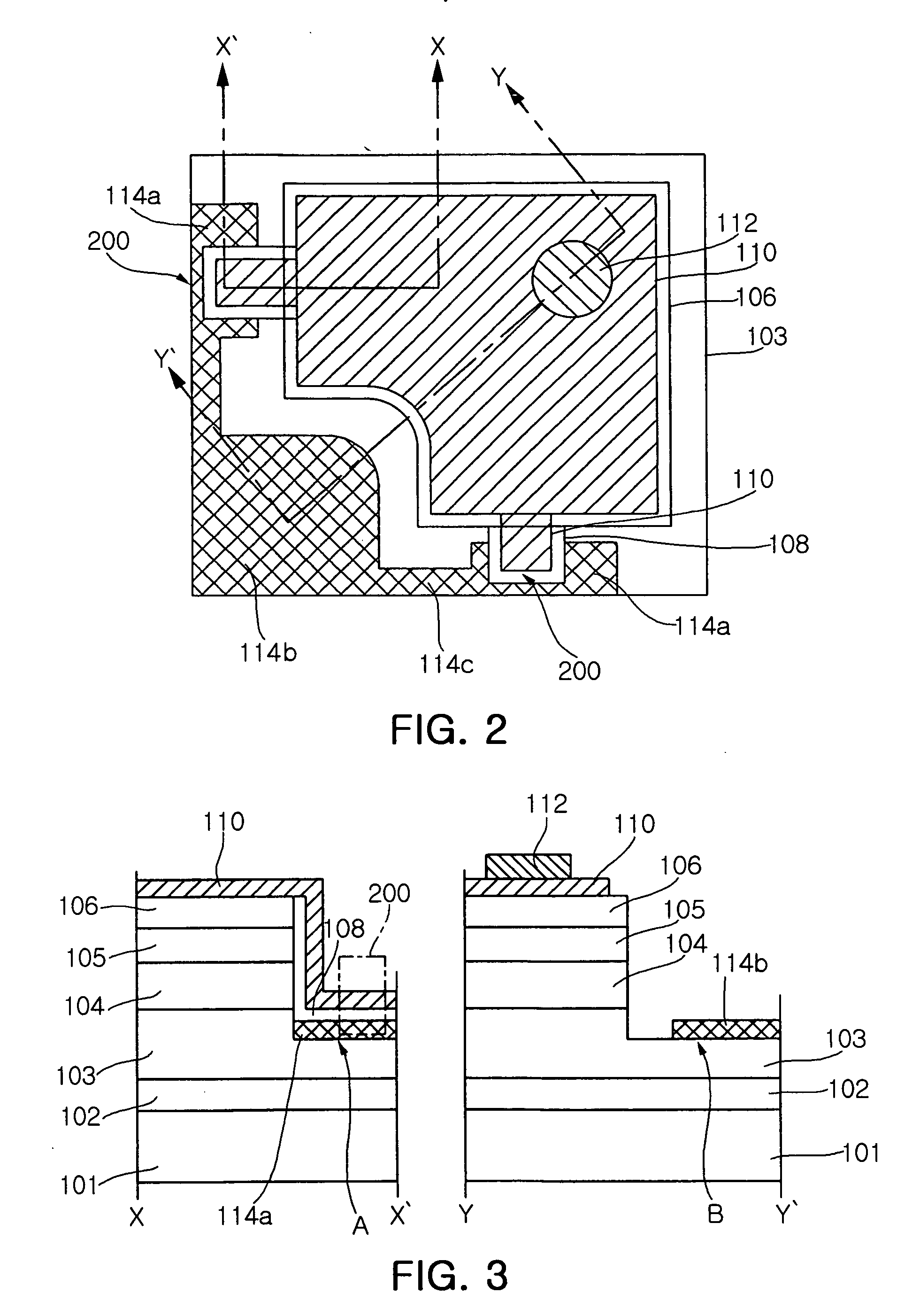
[0037]FIG. 2 is a plan view schematically illustrating a gallium nitride-based light emitting device 300 according to one embodiment of the invention, and FIG. 3 is cross-sectional views taken along lines X-X′ and Y-Y′ of FIG. 2. Referring to FIGS. 2 and 3, the light emitting device 300 comprises a buffer layer 102, an n-type GaN layer 103, ...


PUM


Abstract

A gallium nitride-based light emitting device, and a method for manufacturing the same are disclosed. The light emitting device comprises an n-type GaN-based clad layer, an active layer, a p-type GaN-based clad layer and a p-side electrode sequentially stacked on a substrate. The device further comprises an n-side electrode formed on one region of the n-type GaN-based clad layer, and two or more MIM type tunnel junctions formed on the other regions of the n-type GaN-based clad layer. Each of the MIM type tunnel junctions comprises a lower metal layer formed on the GaN-based clad layer so as to contact the n-type GaN-based clad layer, an insulating film formed on the lower metal layer, and an upper metal layer formed on the insulating film. The device is protected from reverse ESD voltage, so that tolerance to reverse ESD voltage can be enhanced, thereby improving reliability of the device.

Description

RELATED APPLICATION [0001] The present invention is based on, and claims priority from, Korean Application Number 2005-0005138, filed Jan. 19, 2005, the disclosure of which is incorporated by reference herein in its entirety. BACKGROUND OF THE INVENTION [0002] 1. Field of the Invention [0003] The present invention generally relates to a gallium nitride-based light emitting device and a method for manufacturing the same, and, more particularly, to a gallium nitride-based light emitting device, designed to have enhanced tolerance to reverse electrostatic discharge (ESD), and a method for manufacturing the same. [0004] 2. Description of the Related Art [0005] Generally, a conventional gallium nitride-based light emitting device comprises a buffer layer, an n-type GaN-based clad layer, an active layer, and a p-type GaN-based clad layer sequentially stacked on a dielectric sapphire substrate in this order. Additionally, a transparent electrode and a p-side electrode are sequentially form...

Claims


Application Information

Patent Timeline
Patent Type & Authority Applications(United States)
IPC IPC(8): H01L31/12H01L27/15H01L33/06H01L33/32H01L33/38H01L33/42H01L33/44
CPCH01L27/0248H01L27/15H01L33/04H01L33/32H01L33/38H01L33/44H01L2933/0016E01C15/00E01C1/002
Inventor SEO, JUN HOYOON, SUK KILCHAE, SEUNG WAN
Owner SAMSUNG ELECTRONICS CO LTD
Why Eureka
Try Eureka