
Liquid crystal display device
- Summary
- Abstract
- Description
- Claims
- Application Information
AI Technical Summary
Benefits of technology
Problems solved by technology
Method used
Image

Examples
first embodiment
Entire Structure
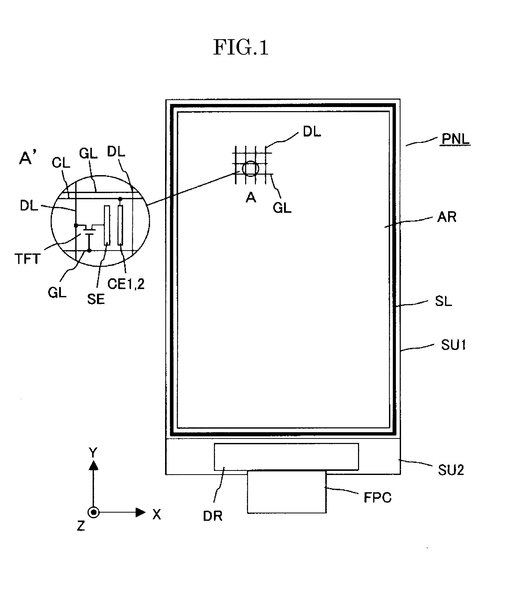
[0068]FIG. 1 is a diagram for illustrating the entire structure of the liquid crystal display device according to the first embodiment of the present invention. In the following, the entire structure of the liquid crystal display device according to the first embodiment is described in reference to FIG. 1. In the present specification, the transmittance, excluding the effects of absorption by color filters CF, polarizing plates POL1, POL2 and the like and the effects of the aperture ratio, is regarded as the efficiency in the display mode. Accordingly, the efficiency in the display mode is 100% in the case where the direction of the oscillation of linearly polarized light emitted from the polarizing plate POL1 on the backlight unit side is rotated by 90° when it enters into the polarizing plate POL2 on the display side.
[0069]As shown in FIG. 1, the liquid crystal display device according to the first embodiment has a liquid crystal display panel PNL that is formed of...
second embodiment
[0111]FIG. 11 is a cross-sectional diagram for schematically illustrating the structure of the liquid crystal display panel in the liquid crystal display device according to the second embodiment of the present invention. In the following, the liquid crystal display device according to the second embodiment is described in reference to FIG. 11. Here, the liquid crystal display panel according to the second embodiment has the same structure as in the first embodiment, except the structure of the regions between a pair of wall pixel electrodes SE, that is to say, the portions of the liquid crystal layer LC to which an electrical field is applied. Accordingly, in the following, the structure of the regions between the wall pixel electrodes SE is described in detail. Though the description of the structure of the pixels according to the second embodiment refers to a case of a so-called multi-domain structure where the angles at which the wall pixel electrodes SE are inclined are differe...
third embodiment
[0132]FIG. 18 is a cross-sectional diagram for illustrating the structure of a pixel in the liquid crystal display device according to the third embodiment of the present invention. The liquid crystal display device according to the third embodiment has the same structure as the liquid crystal display device according to the second embodiment, except the structure of the fifth insulating film IL5 formed between wall pixel electrodes SE that are placed in periphery portions of the pixel so as to face each other. Accordingly, in the following, the fifth insulating film IL5 is described in detail.
[0133]As shown in FIG. 18, in the liquid crystal display device according to the third embodiment, the first substrate SU1 has the same structure as that in the first embodiment. The second substrate SU2 has a first insulating film ILL drain lines DL, a second insulating film IL2, wall bases WL and wall pixel electrodes SE formed in this order on the surface on the liquid crystal side. Here, i...
PUM
 Abstract
Description
Claims
Application Information