Method of manufacturing light-emitting device

a technology of light-emitting devices and manufacturing methods, which is applied in the direction of semiconductor/solid-state device manufacturing, semiconductor devices, electrical devices, etc., can solve the problems of reducing cost, unable to obtain the desired light-emitting device, and the reflector is not formed, so as to achieve the effect of reducing manufacturing costs and high-density mounting of light-emitting elements

Active Publication Date: 2013-01-17
TOYODA GOSEI CO LTD
View PDF0 Cites 21 Cited by
  • Summary
  • Abstract
  • Description
  • Claims
  • Application Information

AI Technical Summary

Benefits of technology

[0023]According to one embodiment of the invention, a method of manufacturing a light-emitting device is conducted such that a lattice frame is formed by dispensing a resin on a light-emitting element mounting surface of a plate-shaped substrate and a sealing material is then filled in an opening defined by the lattice frame (i.e., a region surrounding by the lattice frame in a plan view) to seal a light-emitting element mounted on the surface without using a mold as used in JP-A-2010-177329. Thereby, the high-density mounting of light-emitting elements can be attained without using a large-scale facility such as a mold. Therefore, the manufacturing cost can be significantly reduced.

Problems solved by technology

However, the method of manufacturing a light-emitting device using a lead frame disclosed in JP-A-2010-177329 cannot realize the high-density mounting of light-emitting elements on element mounting portions and also requires a large-scale facility using a mold, which impedes cost reduction.
In the method disclosed in JP-A-2010-177329, a reflector is not formed and it is not possible to obtain a light-emitting device having desired light distribution characteristics.

Method used


Image

  • Method of manufacturing light-emitting device
  • Method of manufacturing light-emitting device
  • Method of manufacturing light-emitting device

Examples


first embodiment

[0032]A method of manufacturing a light-emitting device manufactured using an element collective mounting substrate in a first embodiment of the invention will be described in detail in reference to the drawings.

[0033]Overall Structure of Light-Emitting Device

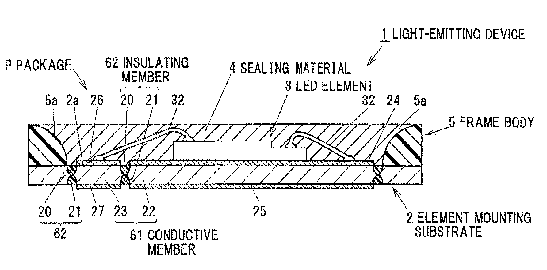
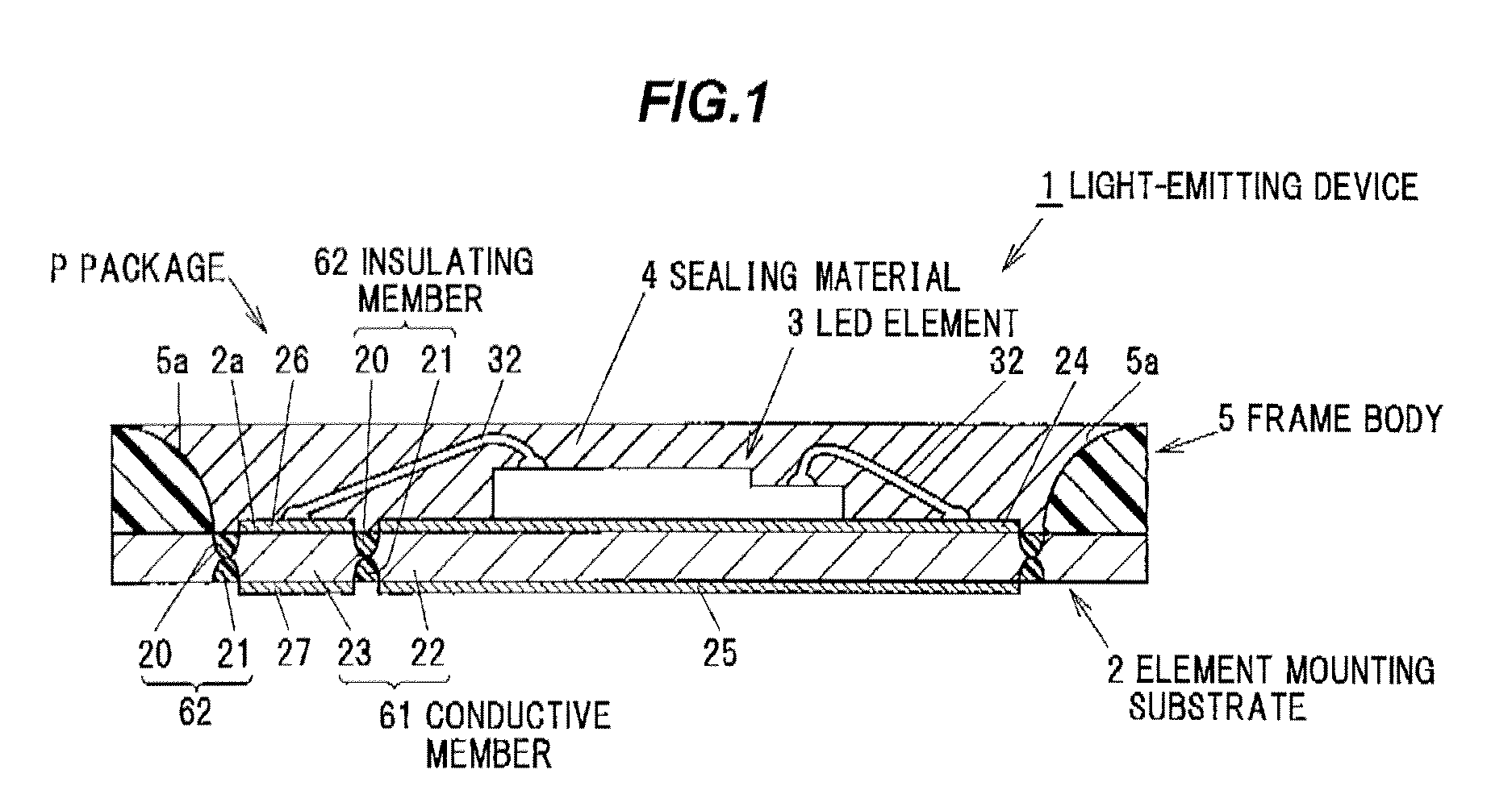
[0034]FIG. 1 shows a light-emitting device. As shown in FIG. 1, a light-emitting device 1 is generally composed of an element mounting substrate 2, an LED element 3 mounted on the element mounting substrate 2, a sealing material 4 for sealing the LED element 3, and a frame body 5 forming a package P together with the sealing material 4 and the element mounting substrate 2.

[0035]Structure of Element Mounting Substrate 2

[0036]The element mounting substrate 2, which is a part of an element collective mounting substrate 6 (shown in FIG. 3) used for manufacturing the light-emitting device 1, has a pair of contact pads 22, 23 as a conductive member which are insulated from each other by a first insulating member 20 and a second insul...

second embodiment

[0074]Next, an element collective mounting substrate and a method of manufacturing a light-emitting device using thereof in a second embodiment of the invention will be described using FIGS. 6A and 6B. FIGS. 6A and 6B show an element collective mounting substrate. In FIGS. 6A and 6B, members which are the same as or equivalent to those in FIGS. 1 to 3B are denoted by the same reference numerals and the explanations thereof will be omitted.

[0075]As shown in FIGS. 6A and 6B, an element collective mounting substrate 9 in the second embodiment of the invention is characterized in that a base material 90 is formed of an insulating member.

[0076]Accordingly, the element collective mounting substrate 9 is composed of a substrate material 9A and a frame assembly 9B each using an insulation material as a base, and is formed entirely of a lattice-shaped composite member to be plural frame bodies 5.

[0077]The substrate material 9A has a base material 90 and a conductive member 91, and is formed ...


PUM


Abstract

A method of manufacturing a light-emitting device includes providing a plate-shaped substrate, forming a lattice frame on a light-emitting element mounting surface of the plate-shaped substrate, mounting a light-emitting device in an opening of the lattice frame on the light-emitting element mounting surface, sealing the light-emitting element by supplying a sealing material into the opening of the lattice frame, and cutting the lattice frame and the plate-shaped substrate so as to split the lattice flame to obtain a plurality of light-emitting devices with a sidewall.

Description

[0001]The present application is based on Japanese patent application No. 2011-155622 filed on Jul. 14, 2011, the entire contents of which are incorporated herein by reference.BACKGROUND OF THE INVENTION[0002]1. Field of the Invention[0003]The invention relates to a method of manufacturing a light-emitting device to obtain plural light-emitting devices by mounting and sealing plural light-emitting elements on an element collective mounting substrate and subsequently dividing the element collective mounting substrate and a frame assembly so as to each include at least one light-emitting element.[0004]2. Related Art[0005]A conventional light-emitting device is provided with an element mounting substrate having an element mounting portion, a light emitting diode (LED) element as a light-emitting element mounted on the element mounting portion of the element mounting substrate, and a sealing material for sealing the LED element.[0006]For manufacturing such a light-emitting device, for e...

Claims


Application Information

Patent Timeline
Patent Type & Authority Applications(United States)
IPC IPC(8): H01L33/48
CPCH01L33/486H01L2933/0033H01L2924/12041H01L2924/07802H01L2224/97H01L24/97H01L2224/49107H01L2224/48247H01L2224/48227H01L2933/005H01L2224/48091H01L2924/00014H01L2224/85H01L2924/00
Inventor TAKEDA, SHIGEOISHIDA, MAKOTOTERAKAMI, MITSUSHIYAMAMORI, SHOTA
Owner TOYODA GOSEI CO LTD
Why Eureka
Try Eureka