Printed wiring board and method of manufacturing the same

a technology of printed wiring and insulating film, which is applied in the direction of lithographic masks, non-metallic protective coating applications, etching metal masks, etc., can solve the problems of no solder resist suitable as insulating film, and no high density mounting can be improved. , to achieve the effect of high temperatur

Inactive Publication Date: 2006-01-17
IBIDEN CO LTD
View PDF32 Cites 11 Cited by
  • Summary
  • Abstract
  • Description
  • Claims
  • Application Information

AI Technical Summary

Benefits of technology

[0027]An operation and effects of the first invention will be explained.
[0028]In the first invention, the entire surface of the insulating substrate is covered with the insulating film and the laser beam is irradiated to a portion for forming th...

Problems solved by technology

However, the above conventional manufacturing method of the printed wiring board 9 has the following problems.
As a result, no high density mounting can be improved.
However, in this method, since the optical curing type resin used as the ...

Method used


Image

  • Printed wiring board and method of manufacturing the same
  • Printed wiring board and method of manufacturing the same
  • Printed wiring board and method of manufacturing the same

Examples


embodiment mode example 1

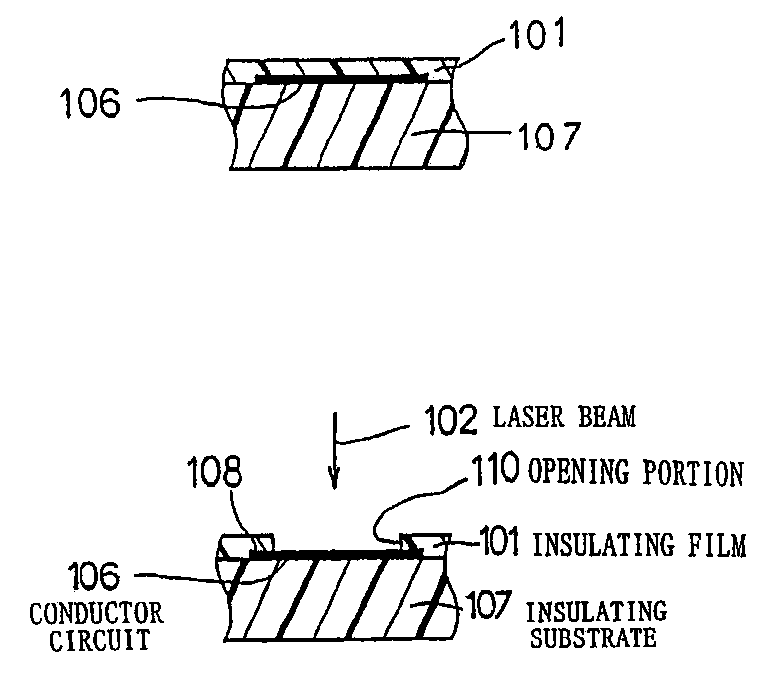
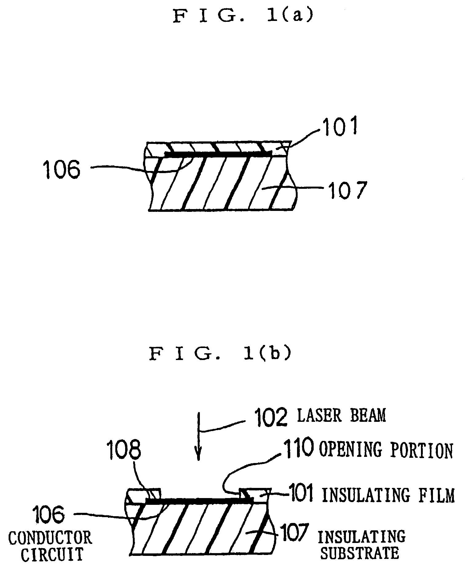
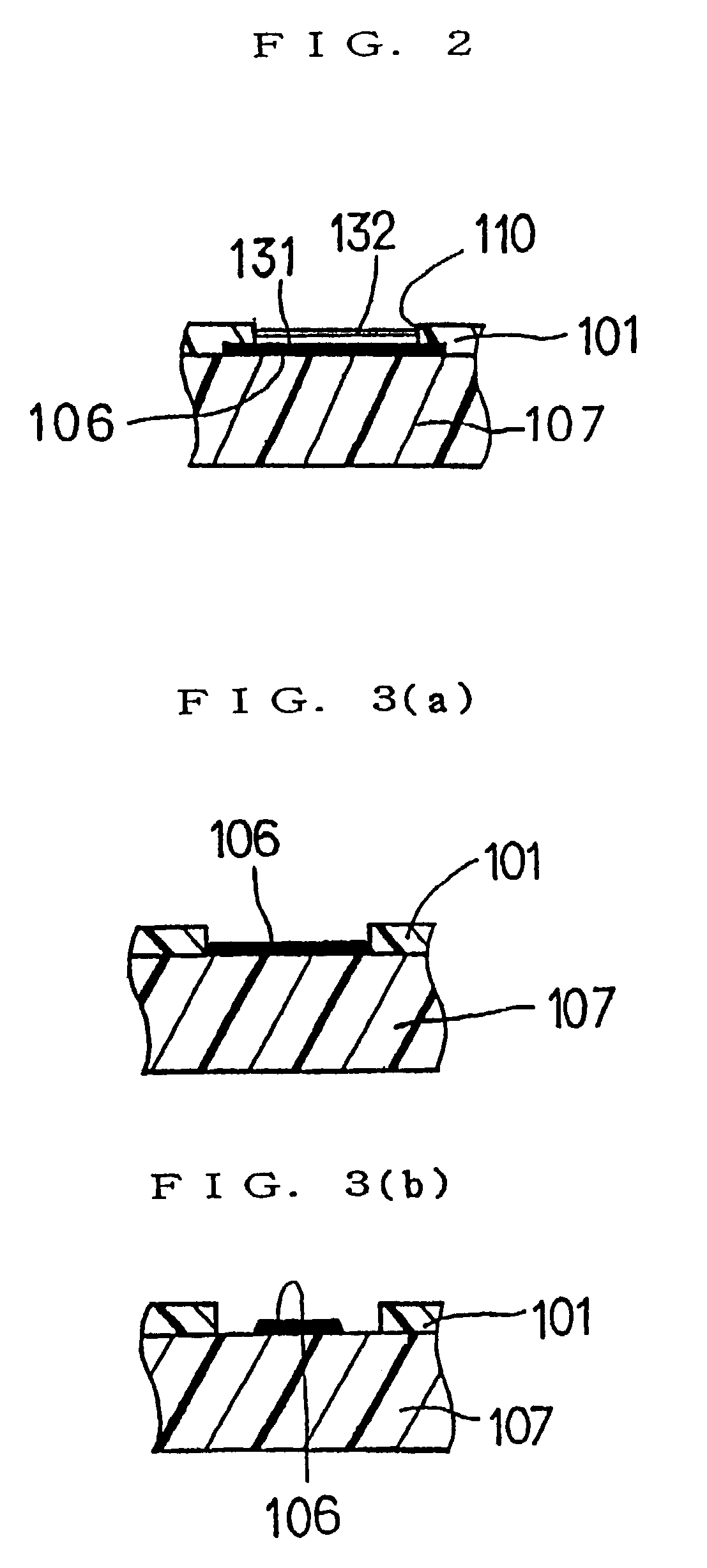
[0165]A manufacturing method of a printed wiring board in an embodiment mode example of a first invention will be explained by using FIGS. 1 to 3.

[0166]A summary of this manufacturing method will first be explained. That is, a solder resist constructed by thermosetting resin is printed on the surface of an insulating substrate 107 having a conductor circuit 106 and including a surface of this conductor circuit 106. The solder resist is thermally cured so that an insulating film 101 having a low coefficient of thermal expansion is formed (FIG. 1(a)). Next, a laser beam 102 is irradiated to an opening portion forming portion in the insulating film 101 and this opening portion forming portion is burnt out, and an opening portion 110 is formed and one portion of the conductor circuit 106 is exposed (FIG. 1(b)).

[0167]A manufacturing method of the above printed wiring board will next be explained in detail.

[0168]First, a copper foil having 18 μm in thickness is stuck to an insulating subs...

embodiment mode example 2

[0182]A printed wiring board in an embodiment mode example of a second invention will be explained by using FIGS. 4 to 7.

[0183]As shown in FIG. 4, the printed wiring board 208 in this example has an upper face pattern 201 formed on an upper face of an insulating substrate 207, a lower face pattern 202 formed on a lower face of the insulating substrate 207, and a hole 203 for conductivity extending through the insulating substrate 207 and reaching an upper face 228 of the lower face pattern 202. A metallic filling material 205 is arranged within the hole 203 for conductivity and is filled with solder for electrically conducting the upper face pattern 201 and the lower face pattern 202. The upper face pattern 201 is covered with a resist film 261 except for a peripheral portion of the hole 203 for conductivity.

[0184]The insulating substrate is set to have 0.1 mm in thickness. As shown in FIG. 5, the hole 203 for conductivity has a diameter A of 0.3 mm. An upper end portion 231 of the ...

embodiment mode example 3

[0197]This example is an embodiment mode example of the second invention. This example differs from the embodiment mode example 2 in that the interior of the hole for conductivity is filled with a metal by a printing method.

[0198]Specifically, similar to the above embodiment mode example 2, after the hole for conductivity is formed, a mask for printing having an opening hole in a portion corresponding to the hole for conductivity is arranged on an upper face side of the insulating substrate. Next, soldering paste is arranged on the mask and is pressed by a roller. Thus, the soldering paste is moved from the opening hole of the mask into the hole for conductivity. Accordingly, the interior of the hole for conductivity is filled with the solder so that a metallic filling material is formed.

[0199]The others are similar to those in the embodiment mode example 2.

[0200]In this example, effects similar to those in the embodiment mode example 2 can be also obtained.


PUM

PropertyMeasurementUnit
Temperature coefficient of resistanceaaaaaaaaaa
Metallic bondaaaaaaaaaa
Thermal expansion coefficientaaaaaaaaaa

Abstract

A solder resist comprising a thermosetting resin is printed on a surface of an insulating board (7) having a conductor circuit (6). The solder resist is then heat-cured to form an insulating film (1) having a low thermal expansion coefficient. A laser beam (2) is then applied to the portion of the insulating film in which an opening is to be formed, to burn off the same portion for forming an opening (10), whereby the conductor circuit (6) is exposed. This opening may be formed as a hole for conduction by forming a metal plating film on an inner surface thereof. It is preferable that an external connecting pad be formed so as to cover the opening. The film of coating of a metal is formed by using an electric plating lead, which is preferably cut off by a laser beam after the electric plating has finished.

Description

CROSS-REFERENCE TO RELATION APPLICATIONS[0001]This is a divisional of allowed application Ser. No. 09 / 891,819 filed Jun. 26, 2001, now U.S. Pat. No. 6,555,208 which is a divisional of application Ser. No. 09 / 348,935 filed Jul. 7, 1999 now U.S. Pat. No. 6,284,353, issued Sep. 4, 2001 which is based upon International Application PCT / JP98 / 00007 filed Jan. 5, 1998, International Publication No. WO 98 / 31204 published Jul. 16, 1998, which is based upon priority Japanese Application 9-14635 filed Jan. 10, 1997; Japanese Application 9-52481 filed Feb. 19, 1997; Japanese Application 9-62131 filed Feb. 28, 1997; Japanese Application 9-65509 filed Mar. 3, 1997; and Japanese Application 9-361961 filed Dec. 9, 1997.BACKGROUND OF THE INVENTION[0002]1. Technical Field[0003]The present invention relates to a printed wiring board and its manufacturing method, and particularly relates to a printed wiring board capable of forming a very small opening portion and a hole for conductivity and be mounted...

Claims


Application Information

Patent Timeline
IPC IPC(8): B05D3/04H05K3/28H01L23/498H05K1/11H05K3/00H05K3/02H05K3/22H05K3/24H05K3/26H05K3/34H05K3/40H05K3/42H05K3/46
CPCH01L23/49816H01L23/49827H01L24/32H05K1/112H05K1/116H05K3/0035H05K3/242H05K3/3452H05K3/4038H01L2224/32057H01L2224/32225H01L2224/48091H01L2224/48227H01L2224/48228H01L2224/73265H01L2224/83385H01L2924/01005H01L2924/01011H01L2924/01029H01L2924/01047H01L2924/01074H01L2924/01078H01L2924/01079H01L2924/01082H01L2924/15153H01L2924/15165H01L2924/15173H01L2924/15311H05K3/0008H05K3/027H05K3/243H05K3/28H05K3/3457H05K3/421H05K3/428H05K3/4602H05K3/4611H05K2201/0305H05K2201/0394H05K2201/09381H05K2201/09509H05K2201/09527H05K2201/0959H05K2201/09781H05K2203/0554H05K2203/0571H05K2203/107H05K2203/175H01L24/48H01L2924/01006H01L2924/01019H01L2924/01033Y10S428/901H01L2924/12041Y10T29/49117Y10T29/49155Y10T29/49165Y10T428/24917H01L2924/00014H01L2924/00H01L2924/00012H01L24/73H01L2924/12042H01L2924/181H01L2224/45099H01L2224/05599H01L2224/85399H01L2224/45015H01L2924/207
Inventor TAKADA, MASARUKOBAYASHI, HIROYUKICHIHARA, KENJIMINOURA, HISASHITSUKADA, KIYOTAKAKONDO, MITSUHIRO
Owner IBIDEN CO LTD
Why Eureka
Try Eureka