Electronic component package and method for producing electronic component package

a technology of electronic components and components, applied in the direction of printed electric component incorporation, printed circuit non-printed electric component association, semiconductor/solid-state device details, etc., can solve the problem of insufficient bonding capability between the conductor post and the electrode pad, and achieve high bonding strength and high density mounting

Inactive Publication Date: 2011-09-22
SUMITOMO BAKELITE CO LTD
View PDF14 Cites 11 Cited by
  • Summary
  • Abstract
  • Description
  • Claims
  • Application Information

AI Technical Summary

Benefits of technology

[0021]In the electronic component package of the present invention, since the back surface side of the circuit board having a conductor post can be a mounting surface, high-density mounting on the mounting surface can be achieved.
[0022]According to the present invention, an adhesive layer for bonding the circuit board and the electronic component contains a flux activating compound, so that the surfaces of the solder layer and the metal layer are reduced because of the compound, and an oxide film cannot be formed. For this reason, the solder layer and the metal layer are well metal-bonded so that the conductor post and the electrode pad can be integrated into one body with a high bonding strength.

Problems solved by technology

However, in a semiconductor package described in the above Patent Document, bonding capability between the conductor post and the electrode pad is not sufficient so that further improvement has been in demand.

Method used


Image

  • Electronic component package and method for producing electronic component package
  • Electronic component package and method for producing electronic component package
  • Electronic component package and method for producing electronic component package

Examples


first embodiment

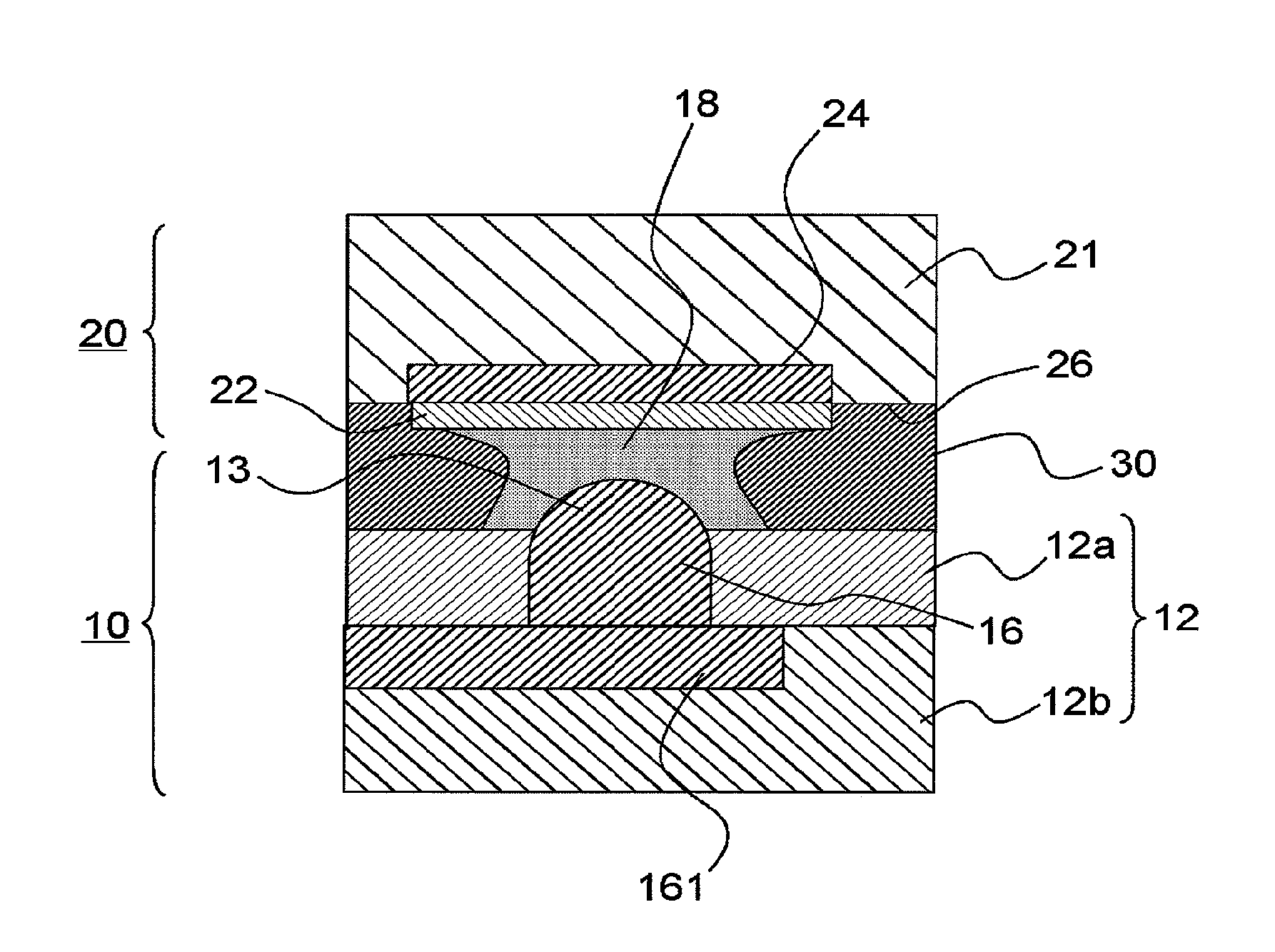
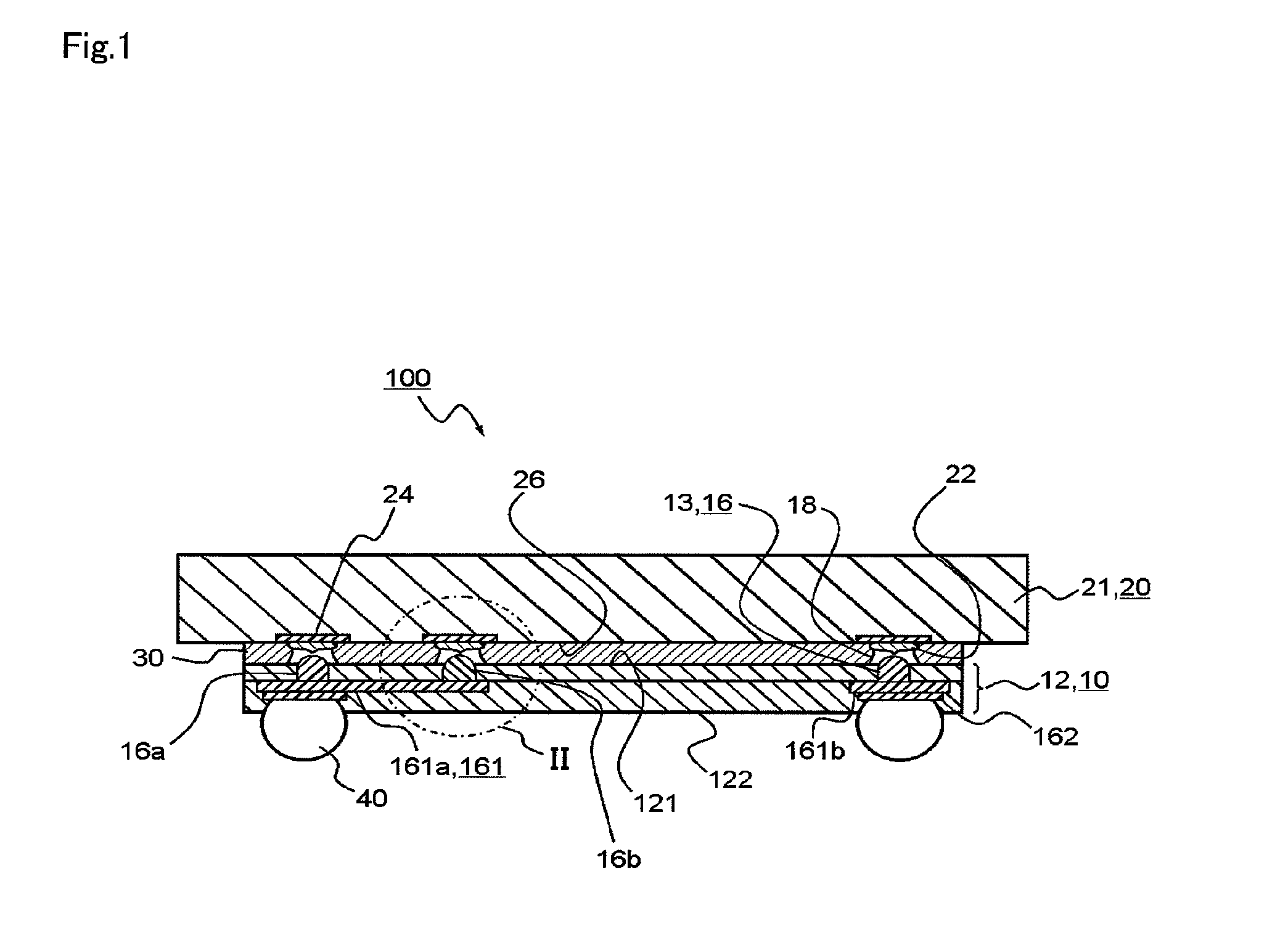
[0033]Electronic Component Package

[0034]FIG. 1 is a laminated cross-sectional view illustrating one example of an electronic component package 100 of a first embodiment of the present invention.

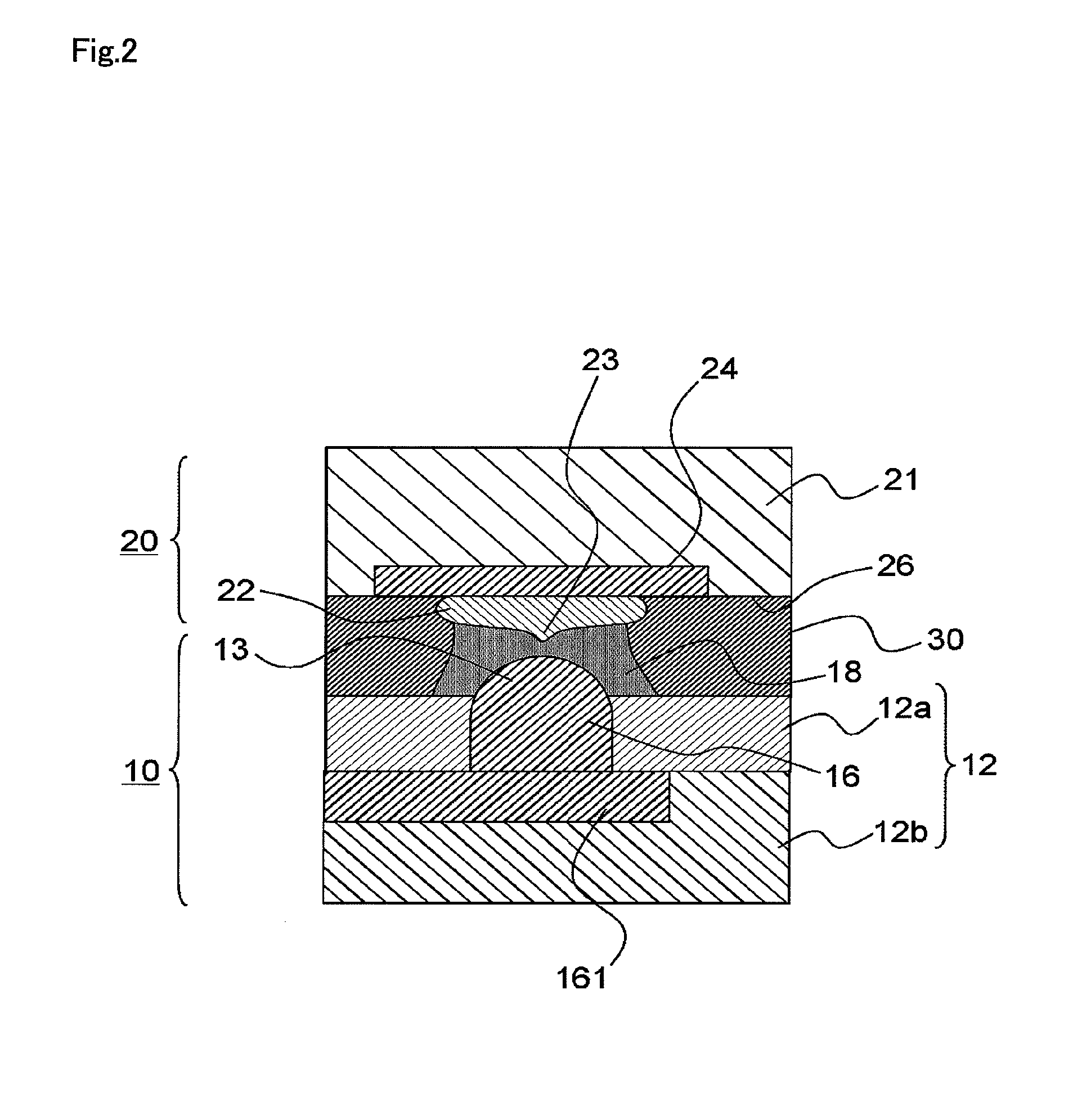
[0035]FIG. 2 is an enlarged view of a region represented by circle II in FIG. 1.

[0036]First, a summary of the electronic component package 100 of this embodiment will be described.

[0037]The electronic component package 100 of this embodiment includes a circuit board 10, an electronic component 20 and an adhesive layer 30.

[0038]The circuit board 10 is provided with a base member 12, an electrically-conductive conductor post 16 which is buried in the base member 12, and a solder layer 18 which is provided at the front end 13 of the conductor post 16 while exposed from a surface 121 of the base member 12.

[0039]The electronic component 20 has an electrode pad 24 having a metal layer 22 mounted thereon provided on a main surface 26 thereof.

[0040]The adhesive layer 30 contains a flux activating com...

second embodiment

[0226]Further, the present invention is not restricted to the aforementioned embodiments, and various modifications, improvements and the like are intended to be included within the scope of the present invention in the ranges in which the object of the present invention can be achieved.

[0227]FIG. 8 is an enlarged cross-sectional view in the vicinity of the conductor post 16 of the electronic component package 100 according to this embodiment. FIG. 8 corresponds to FIG. 2 of the first embodiment.

[0228]This embodiment is different from the first embodiment in that the metal layer 22 mounted on the electrode pad 24 is formed in a film form.

[0229]More specifically, as the metal layer 22 of this embodiment, there may be used a solder plating layer containing at least one kind of a nickel-gold plating layer, an aluminum plating layer, a gold plating layer, a nickel plating layer and a copper plating layer, or tin. The nickel-gold plating layer mentioned herein is a layer with a top layer...


PUM

PropertyMeasurementUnit
thicknessaaaaaaaaaa
temperatureaaaaaaaaaa
electrically-conductiveaaaaaaaaaa

Abstract

Disclosed is an electronic component package 100 including a circuit board 10, an electronic component 20, and an adhesive layer 30. The circuit board 10 is provided with an electrically-conductive conductor post 16 which is buried in a base member 12, and a solder layer 18 which is provided at the front end 13 of the conductor post 16 while exposed from a surface 121 of the base member 12. An electrode pad 24 having a metal layer 22 mounted thereon is provided on the main surface 26 of the electronic component 20. The adhesive layer 30 contains a flux activating compound, and bonds the surface 121 of the base member 12 and the main surface 26 of the electronic component 20. Then, the metal layer 22 and the solder layer 18 are metal-bonded.

Description

TECHNICAL FIELD[0001]The present invention relates to an electronic component package and a method for producing the electronic component package.BACKGROUND ART[0002]With the recent requirements of higher functionality and reduction in weight and size of electronic equipments, high-density integration and high-density mounting of electronic components are in progress.[0003]With respect to this technology, the following Patent Document 1 discloses an invention of a semiconductor package in which a plating layer made of gold or nickel is provided on a surface of a conductor post protruding from an interposer substrate, and such a conductor post is bonded to an electrode pad formed on a semiconductor chip.RELATED DOCUMENTPatent Document[0004]Patent Document 1: Japanese Patent Application Laid-Open No. 2008-153482DISCLOSURE OF THE INVENTION[0005]However, in a semiconductor package described in the above Patent Document, bonding capability between the conductor post and the electrode pad...

Claims


Application Information

Patent Timeline
Patent Type & Authority Applications(United States)
IPC IPC(8): H05K1/09H05K3/00H05K1/18H05K1/02
CPCH01L23/49816Y10T29/49124H01L24/81H01L24/97H01L2221/68331H01L2221/68336H01L2224/1134H01L2224/131H01L2224/16H01L2224/81192H01L2224/81193H01L2224/812H01L2224/81801H01L2224/83192H01L2224/97H01L2924/01004H01L2924/0101H01L2924/01013H01L2924/01015H01L2924/01027H01L2924/01029H01L2924/0103H01L2924/01033H01L2924/01047H01L2924/01049H01L2924/01051H01L2924/01075H01L2924/01078H01L2924/01079H01L2924/01082H01L2924/15311H01L2924/19041H01L24/16H01L2924/014H01L2924/01006H01L2924/01005H01L2924/00013H01L2224/13109H01L2224/81H01L2224/13099H01L2924/351H01L2924/12042H01L2224/73104H01L2924/00H01L23/48H01L23/12
Inventor CHUMA, TOSHIAKIKONDO, MASAYOSHITANAKA, SATOSHIKANEMASA, KENICHI
Owner SUMITOMO BAKELITE CO LTD
Why Eureka
Try Eureka