Integrated circuit and layered circuit provided therewith

a technology of integrated circuits and layers, applied in the direction of inductance, pulse technique, semiconductor/solid-state device details, etc., can solve the problems of high density/high integration of semiconductor devices, and achieve the effect of preventing cross-talk between adjacent coils and high density

Active Publication Date: 2016-06-02
THRUCHIP JAPAN INC
View PDF6 Cites 12 Cited by
  • Summary
  • Abstract
  • Description
  • Claims
  • Application Information

AI Technical Summary

Benefits of technology

[0014]According to an aspect of the present invention, cross-talk between adjacent coils can be prevented and coils can be mounted with high density.

Problems solved by technology

However, the use of wiring makes high-densification / high integration of the semiconductor device difficult.

Method used


Image

  • Integrated circuit and layered circuit provided therewith
  • Integrated circuit and layered circuit provided therewith
  • Integrated circuit and layered circuit provided therewith

Examples


Embodiment Construction

[0022]In the following, embodiments of the present invention are described with reference to the accompanying drawings.

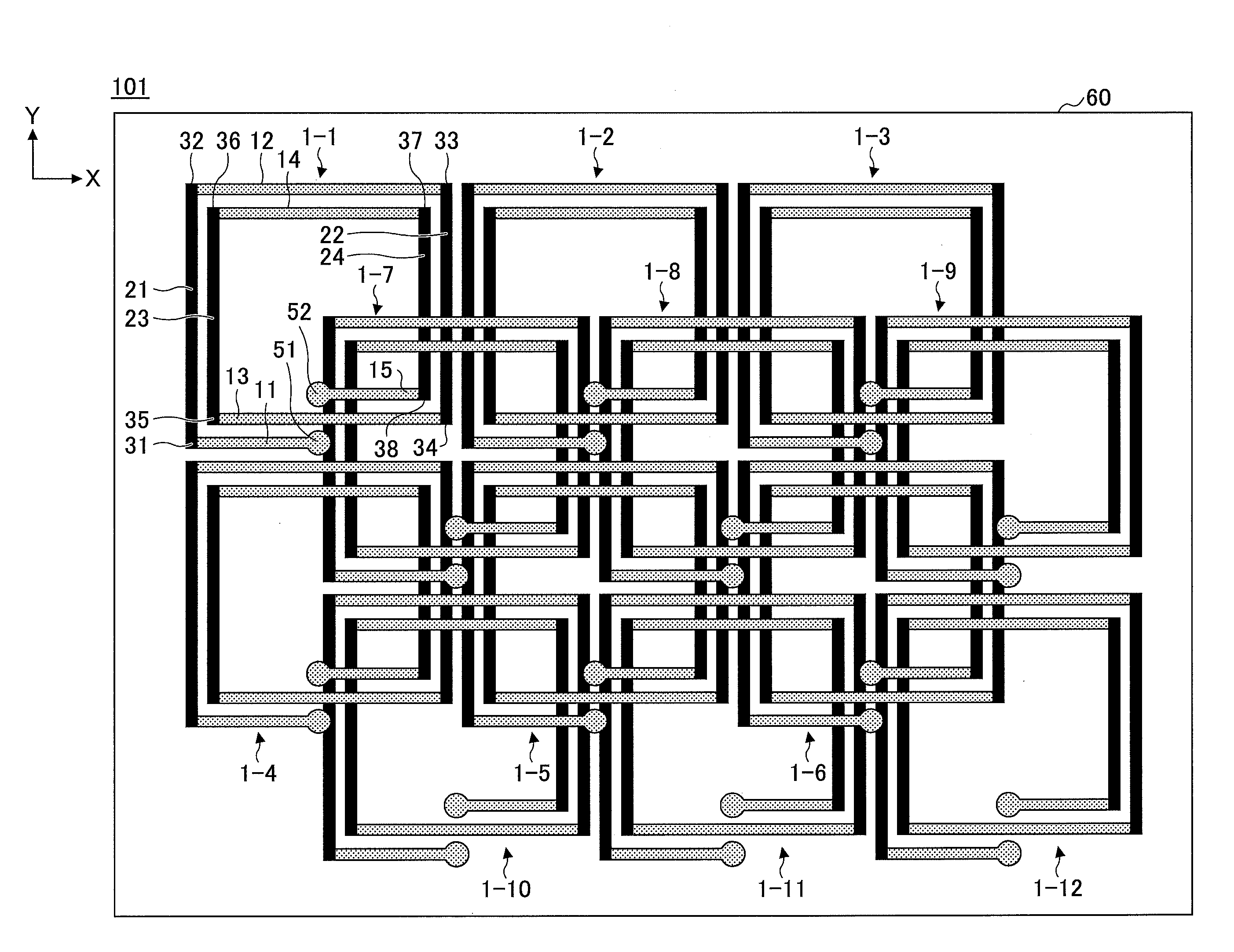
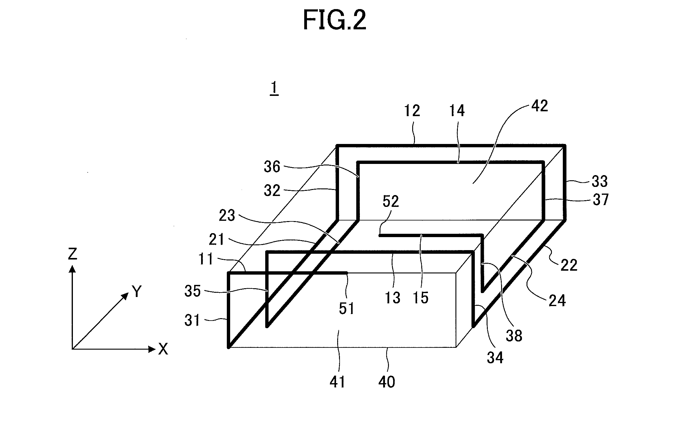
[0023]FIG. 1 is a schematic diagram illustrating an exemplary configuration of a semiconductor integrated circuit 101. The semiconductor integrated circuit 101, which is an example of an integrated circuit, includes a substrate 60 and multiple coils formed on the substrate 60. Twelve coils 1-1 to 1-12 are illustrated in FIG. 1. Note that the outer shape and area of the substrate 60 is discretional.

[0024]The coils 1-1 to 1-12 have quadrate shapes and include first and second wiring that are alternately connected to each other and formed on different layers in a perpendicularly intersecting manner. In FIG. 1, for example, a first wiring that is formed on a first layer is illustrated with a black solid line, and a second wiring is formed on a second layer (different from the first layer) in a manner perpendicularly intersecting the first wiring and is illustrated with ...


PUM


Abstract

An integrated circuit includes multiple quadrangular coils including a first wiring and a second wiring that are alternately connected to each other and formed on different layers in a manner perpendicularly intersecting each other. The coils are partly overlapped with each other in a diagonal direction that connects opposite corners of the coils. The coils preferably have the same structures. A target coil among the coils preferably partly overlaps with another coil among the coils in two diagonal directions that connect opposite corners of the target coil.

Description

TECHNICAL FIELD[0001]The present invention relates to an integrated circuit and a layered circuit provided therewith.BACKGROUND ART[0002]In recent years, a large capacity layered-type semiconductor memory device having multiple semiconductor memories layered thereon is developed to allow the semiconductor memory device to be controlled from outside in the same manner as controlling a single semiconductor memory. For example, a Solid State Drive (SSD) using a non-volatile memory instead of a magnetic hard disk can have its memory capacity increased by layering multiple flash memory chips of the same kind.[0003]The connection and power supply between the chips of the layered-type semiconductor memory device may be performed, for example, by using wirings. However, the use of wiring makes high-densification / high integration of the semiconductor device difficult.[0004]Thus, technology for wirelessly connecting multiple layers of chips and multiple layers of printed circuit boards in a l...

Claims


Application Information

Patent Timeline
Patent Type & Authority Applications(United States)
IPC IPC(8): H04B5/00H01L23/528H01L23/522
CPCH04B5/0081H04B5/0031H01L23/5283H01L23/5227H01F27/2804H01F2027/2809H01L2924/0002H01L2924/00H01F17/00H01F27/00H03K19/00
Inventor KURODA, TADAHIRO
Owner THRUCHIP JAPAN INC
Why Eureka
Try Eureka