Apparatus and Method for Guiding Optical Waves

a technology of optical waves and apparatus, applied in the field of optical communication devices, can solve the problem that the geometry of optical waves cannot be changed anymor

Active Publication Date: 2013-02-07
FRAUNHOFER GESELLSCHAFT ZUR FOERDERUNG DER ANGEWANDTEN FORSCHUNG EV
View PDF0 Cites 22 Cited by
  • Summary
  • Abstract
  • Description
  • Claims
  • Application Information

AI Technical Summary

Benefits of technology

[0012]According to another embodiment, a method for variably guiding optical waves may have the steps of activating an electro-optic effect in a region of an electro-optic core layer of electro-optic material by an electric field generated by means of an electrode arrangement with at least a first electrode layer in proximity to the electro-optic core layer, such that a propagation of the light is manipulated in the region of the activated electro-optic effect, wherein the first electrode layer has a regular two-dimensional array of planar arranged and individually addressable first electrodes to activate the electro-optic effect in the region of the electro-optic core layer by an electric field generated by individually applying electric potentials to addressed first electrodes, and wherein the electrode arrangement has, arranged in proximity and on a same side of the electro-optic core layer as the first electrode layer, a further electrode layer in parallel to the first electrode layer, the further electrode layer having a plurality of individually addressable further electrodes, arranged such that a position of a further electrode laterally intermediates positions of two neighbouring first electrodes in order to minimize electrical field inhomogeneities due to lateral electrode separation, wherein the region, in which the electro-optic effect is activated, represents an optical pathway permitting propagation of light such that the shape of the optical pathway is determined by the pattern of addressed electrodes.
[0013]It is the finding of the present invention that a waveguide geometry or an optical pathway may be varied by using a layer stack of planar arranged electro-optically active materials and an electrode arrangement with at least one electrode layer in proximity to the electro-optically active layer stack. By freely programming or selecting individual electrodes of the electrode arrangement it is possible to generate various waveguide structures or optical pathways by selecting corresponding electrode pathways.
[0021]Hence, by using embodiments of the present invention, it is possible to design a variable or variably configurable planar electro-optic waveguide device that comprises a multi-layer system having a core layer of electro-optic material and a passive or an electro-optic cladding layer, wherein the refractive index of the cladding is lower than or equal to the refractive index of the core layer for confining light in the core layer by total reflection. The electro-optic effect is activated in a region of the core layer by applying a corresponding electric field across it, i.e., applying corresponding electric potentials on electrodes of electrode layers placed in the proximity of the multi-layer system. At least one of the electrode layers, macroscopic in size, is patterned such that a plurality of closely packed, identically shaped individual flat sub-electrodes, microscopic in size, is formed. Thereby, the sub-electrodes are arranged in one- or two-dimensional arrays and are placed in a same plane. The microscopic sub-electrodes will also be referred to as “pixel electrodes” on a “pixelized planar surface” in the sequel of this specification. This pixelized planar surface of the electrode layer may be placed on a substrate made of, e.g., silicon or glass. The pixel electrodes may be contacted separately via the substrate by any known means, such that they are individually addressable. This may be achieved by integrating the pixel electrodes in an active matrix, e.g., a SRAM-like architecture or, passively, i.e., one electrical connection per pixel electrode to a driver electronics. A geometrical shape of the pixel electrodes and / or a distance between them is advantageously chosen so that to assure a maximum surface coverage and to best fit the shape of any waveguide device or any combination of various waveguide devices.

Problems solved by technology

A drawback of conventional waveguide devices and methods for their fabrication is that once the waveguide materials are structured, their geometry cannot be changed anymore.

Method used


Image

  • Apparatus and Method for Guiding Optical Waves
  • Apparatus and Method for Guiding Optical Waves
  • Apparatus and Method for Guiding Optical Waves

Examples


Embodiment Construction

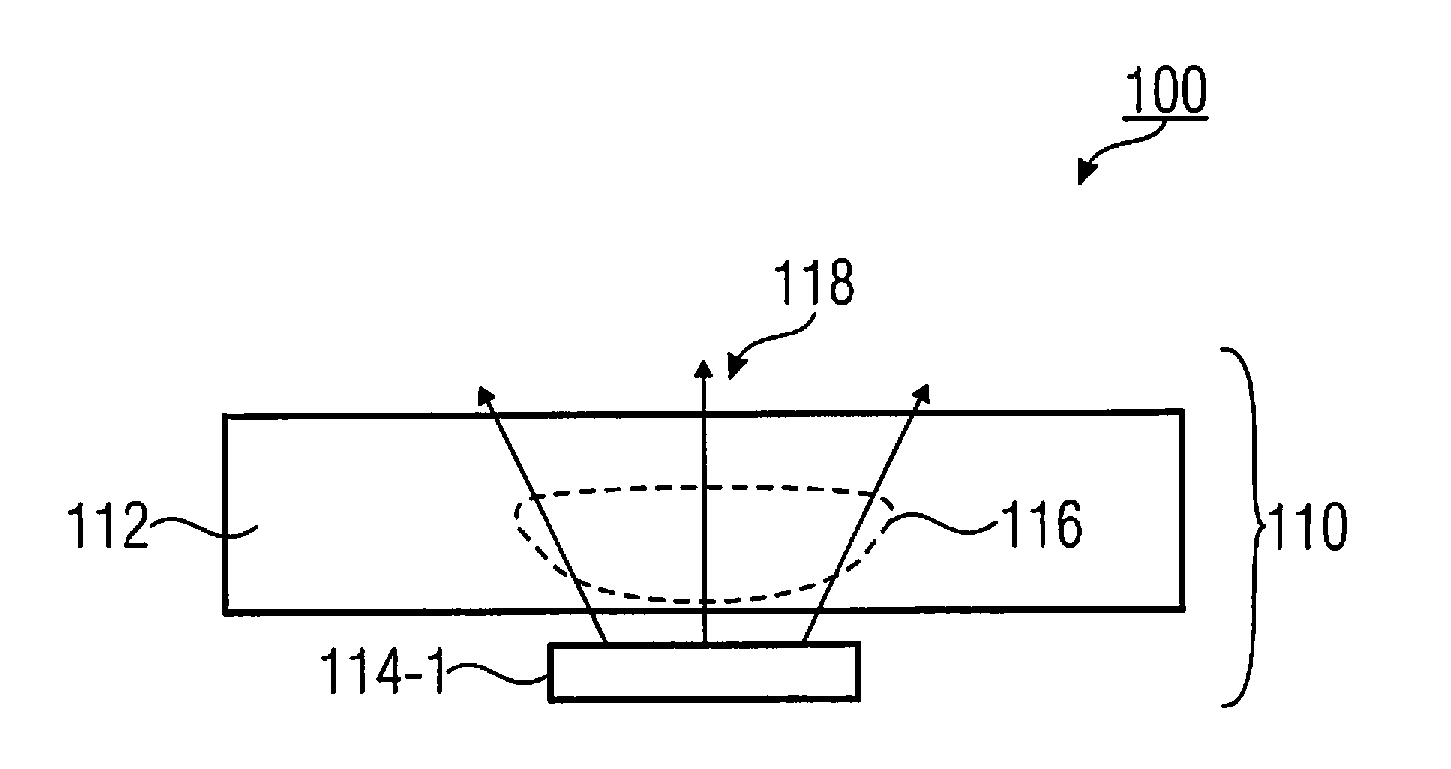
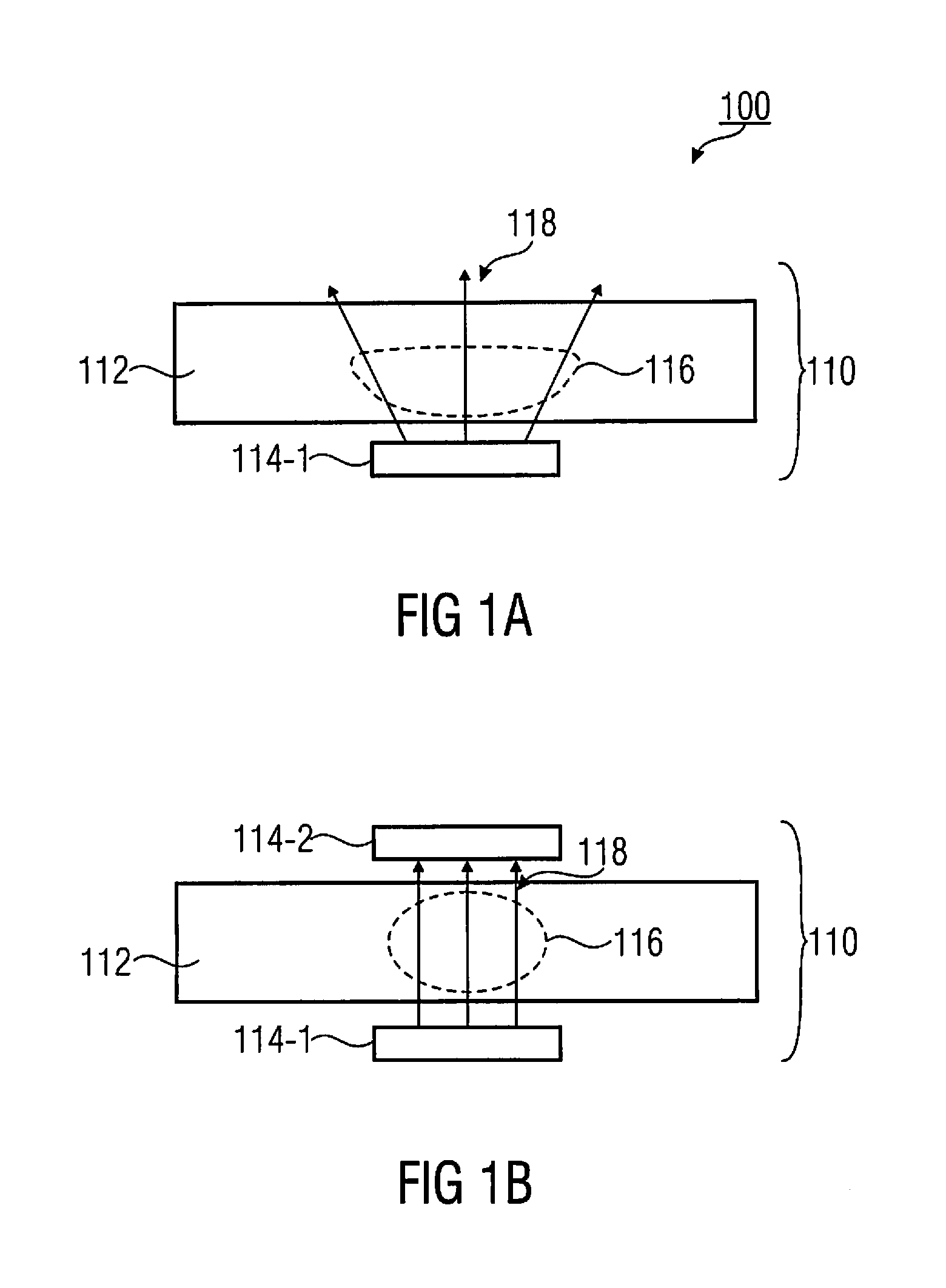
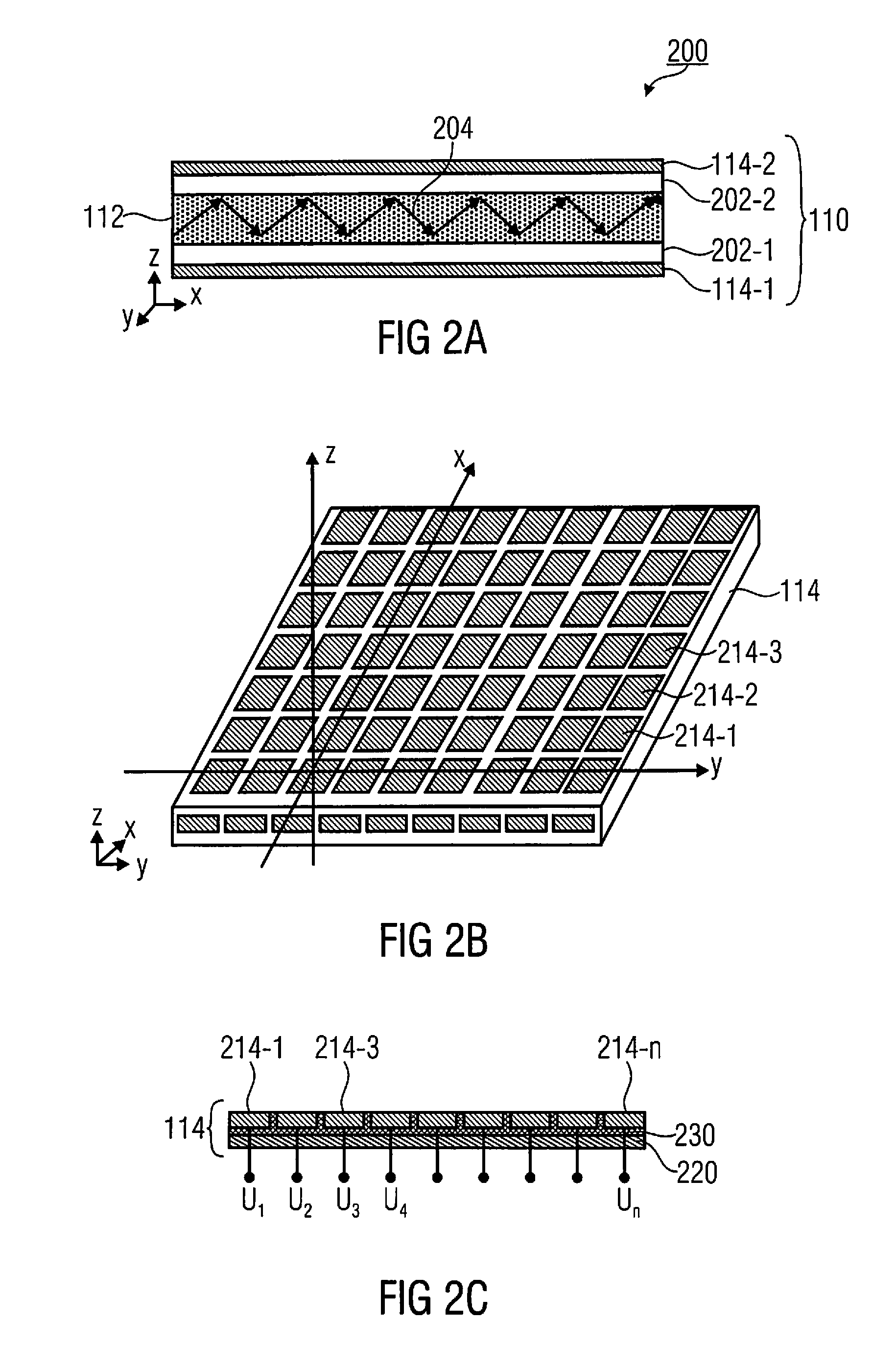
[0045]In optical communication systems fast modulation and switching of optical signals as well as sub-nanosecond switching times are important functions. One effect that can be exploited successfully to obtain such functionalities is the electro-optic (EO) effect, which occurs in some materials. The electro-optic effect is a change in the optical properties of a material in response to an electric field. In an uniaxial (i.e., if the material has a single axis of anisotropy or optical axis) birefringent (i.e., decomposition of a ray of light into two rays, the ordinary ray and the extraordinary ray, when it passes through certain types of material) electro-optic material a refractive index change induced by a modulating external electric field is given by:

Δn=½n03rE+½n03RE2+  (2)

[0046]wherein the first term ½n03rE of the right side describes the so-called Pockels effect or linear electro-optic effect, which occurs in some non-centrosymmetric materials, while the second term ½n03RE2 o...


PUM

PropertyMeasurementUnit
electric fieldaaaaaaaaaa
electric potentialsaaaaaaaaaa
electrical field inhomogeneitiesaaaaaaaaaa

Abstract

Provided is a concept for variably guiding optical waves by using a layer-stack having an electro-optic core layer of electro-optic material for guiding light and an electrode arrangement with at least a first electrode layer in proximity to the electro-optic core layer, wherein the electrode arrangement is configured to activate an electro-optic effect in a region of the electro-optic core layer by an electric field generated by means of the electrode arrangement, such that a propagation of the light is manipulated in the region of the activated electro-optic effect.

Description

CROSS-REFERENCE TO RELATED APPLICATIONS[0001]This application is a continuation of copending International Application No. PCT / EP2010 / 051722, filed Feb. 11, 2010, which is incorporated herein by reference in its entirety.BACKGROUND OF THE INVENTION[0002]The present invention generally relates to optical communication devices and, in particular, to variably configurable optical waveguide devices (VOWD).[0003]Optical telecommunication networks over large distances include a wide variety of devices for routing, splitting, interconnecting, modulating and amplifying electromagnetic radiation at optical frequencies, i.e. light. Planar devices such as connectors, switches, power attenuators, beam steerers, directional couplers and intensity modulators, etc., incorporate passive and / or active optical waveguides as basic transport means for an encoded light wave.[0004]There are a variety of passive and (electro-optically) active waveguide structures. Waveguides used at optical frequencies ar...

Claims


Application Information

Patent Timeline
Patent Type & Authority Applications(United States)
IPC IPC(8): G02F1/295
CPCG02F1/313G02F2201/122G02F1/035G02F1/0316
Inventor COSTACHE, FLORENTABLASL, MARTINSCHENK, HARALD
Owner FRAUNHOFER GESELLSCHAFT ZUR FOERDERUNG DER ANGEWANDTEN FORSCHUNG EV
Why Eureka
Try Eureka