Method for producing a deep trench in a microelectronic component substrate

a microelectronic component and substrate technology, applied in the direction of basic electric elements, semiconductor/solid-state device manufacturing, electric devices, etc., can solve the problems of large defect source in the trench, affecting the operation of the components, and affecting the quality of the components, so as to prevent any over-etching phenomenon, less aggressive, and control the profile of the etched portion more accurately

Active Publication Date: 2013-02-28
STMICROELECTRONICS (CROLLES 2) SAS
View PDF3 Cites 6 Cited by
  • Summary
  • Abstract
  • Description
  • Claims
  • Application Information

AI Technical Summary

Benefits of technology

This patent describes a method for creating shallow trenches in semiconductor devices. A new technique called plasma-based ion etching has been developed which allows for precise control over the shape of the etched area. By applying two different levels of etching, one at high power and another at low power, the method prevents damage to the surrounding materials and ensures a smooth surface. This results in improved performance and reliability of the finished device.

Problems solved by technology

The technical problem addressed in this patent text is the need for an etch method that can produce deep trenches with low form factors and smooth sidewalls, free of surface defects. Existing methods have limitations such as slow speed or irregular sidewalls, which hinder subsequent treatment and production of microelectronic components.

Method used


Image

  • Method for producing a deep trench in a microelectronic component substrate
  • Method for producing a deep trench in a microelectronic component substrate
  • Method for producing a deep trench in a microelectronic component substrate

Examples


Embodiment Construction

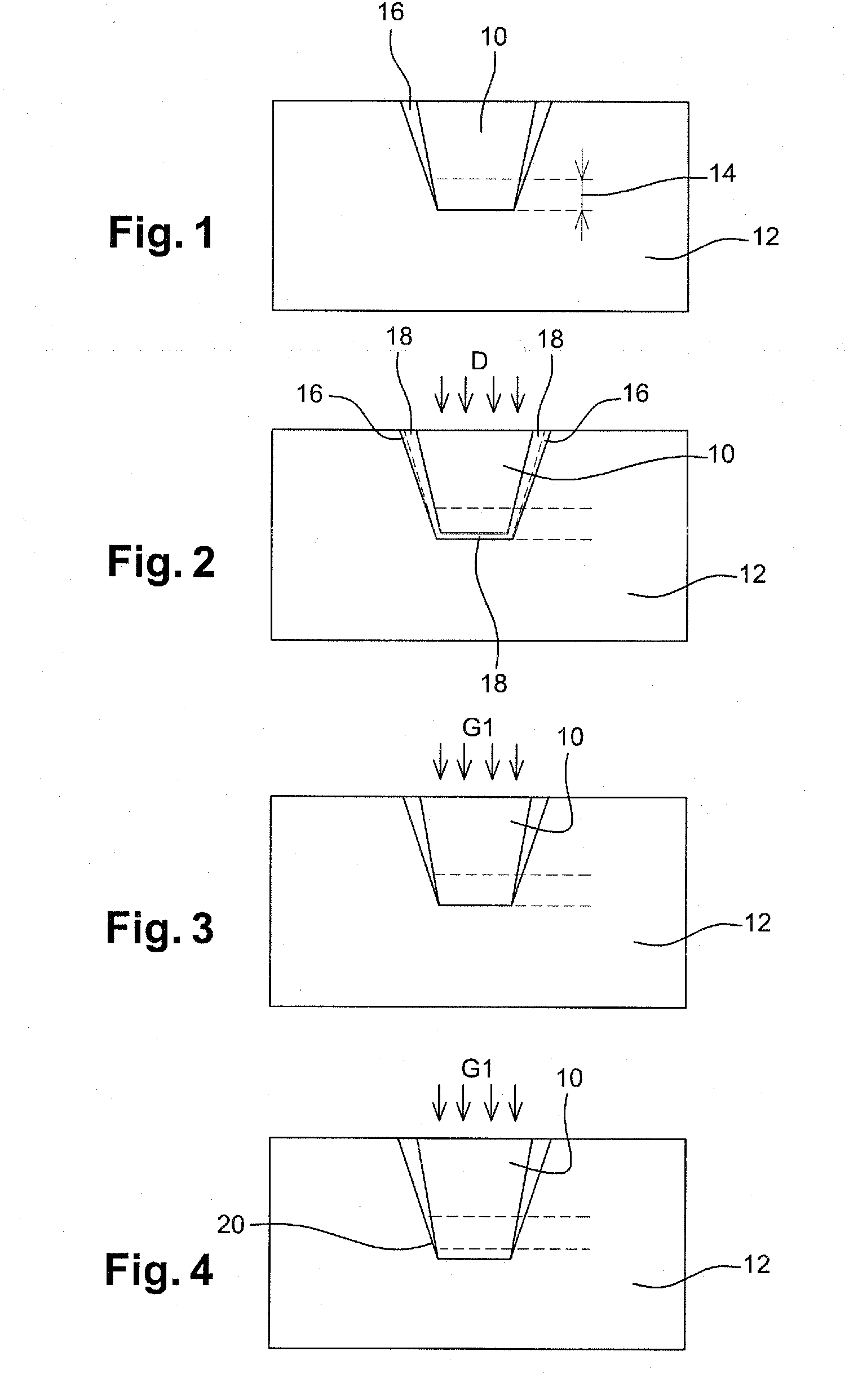
[0035]An inventive embodiment will now be described in relation to FIGS. 1 to 5, the various layers having been deliberately exaggerated in the interests of greater clarity.

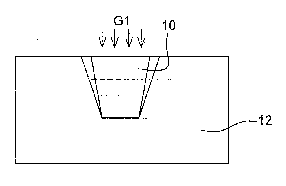
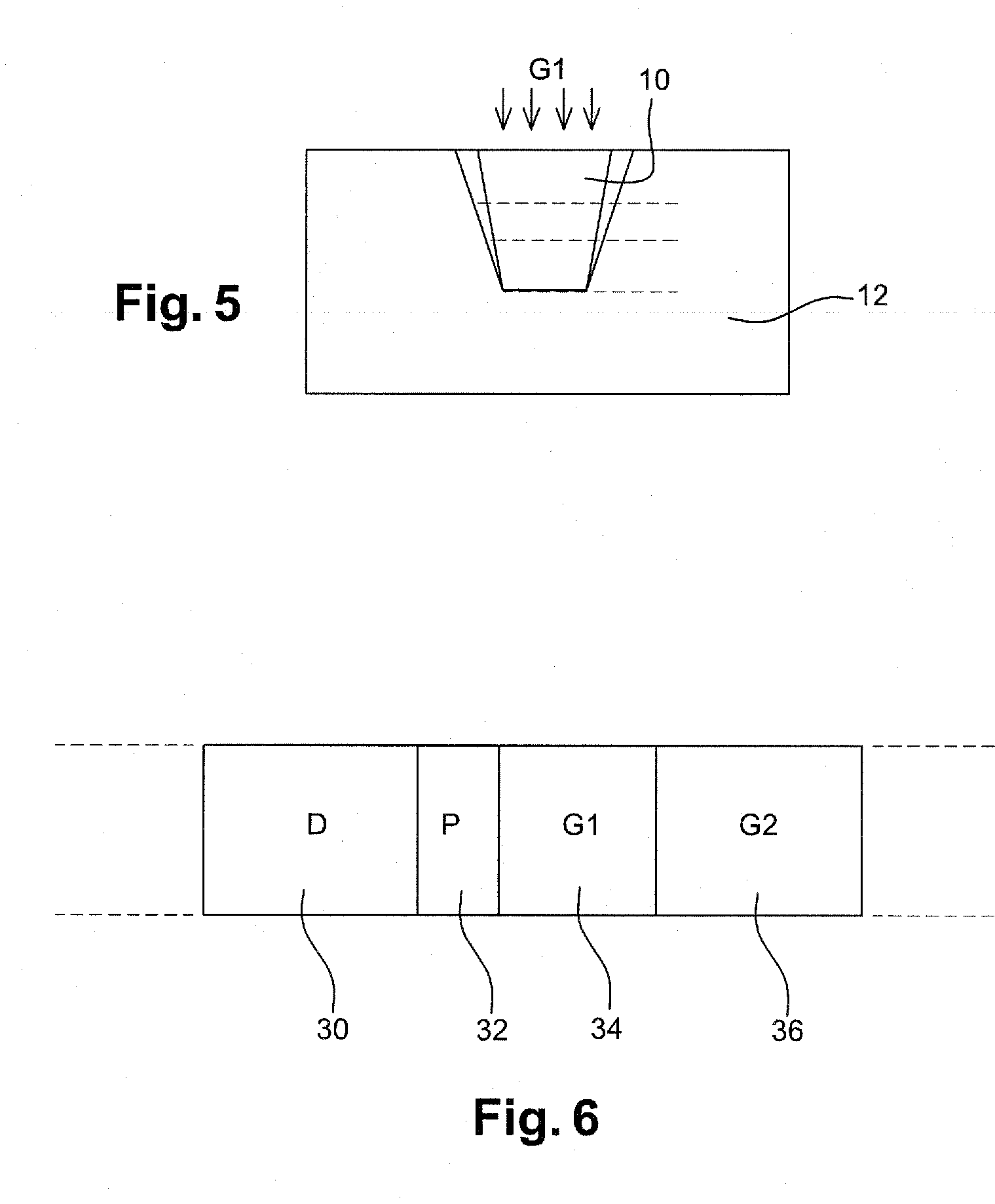
[0036]The method comprises a series of elementary etch cycles, each etching a portion of a trench 10 produced in a substrate 12, for example a semi-conductor substrate, in particular of silicon.

[0037]FIG. 1 shows the result obtained at the end of previous elementary cycles, the result of the last elementary cycle 14 being shown between the dotted lines. In particular, the trench 10 is coated with a passivation layer 16 of decreasing thickness.

[0038]An elementary cycle starts with the deposition of a new passivation layer 18 in the trench 10. For example, a plasma is used with only a fluorocarbon gas which deposits a carbon- and fluorine-based polymer on the side walls and the bottom of the trench 10 (FIG. 2). The passivation layer deposited 18 is to advantage constituted by fluorocarbon, and comes, for example, f...


PUM


Abstract

A method for producing a deep trench in a substrate includes a series of elementary etch cycles each etching a portion of the trench. Each elementary cycle includes deposition of a passivation layer on the sidewalls and the bottom of the trench portion etched during previous cycles; followed by pulsed plasma anisotropic ion etching of the trench portion etched during previous cycles, the etching; being implemented in an atmosphere comprising a passivating species; and including a first etch sequence followed by a second etch sequence of less power than the power of the first etch sequence. The first etch sequence etches the passivation layer deposited in the bottom of the portion so as to access the substrate and etches the free substrate at the bottom of the portion while leaving a passivation layer on sidewalls of the portion.

Description


Claims


Application Information

Patent Timeline
Owner STMICROELECTRONICS (CROLLES 2) SAS
Why Eureka
Try Eureka