Display panel and method of manufacturing the display panel

a technology of display panel and display panel, which is applied in the manufacture of electrode systems, electric discharge tubes/lamps, instruments, etc., can solve the problems of poor video characteristic, low response speed, and difficult improvement of display quality of 3-dimensional (“3d”) images, and achieve the effect of improving response speed

Active Publication Date: 2013-03-28
SAMSUNG DISPLAY CO LTD +1
View PDF6 Cites 25 Cited by
  • Summary
  • Abstract
  • Description
  • Claims
  • Application Information

AI Technical Summary

Benefits of technology

[0011]Exemplary embodiments of the present invention prov

Problems solved by technology

Since a typical liquid crystal display (“LCD”) panel is driven by a driving method of a hold type, a video characteristic may be poor compared to a traditional cathode-ray tube (“CRT”) display device.
In addition, a response speed may be low so that a display quality of a 3-dimensio

Method used


Image

  • Display panel and method of manufacturing the display panel
  • Display panel and method of manufacturing the display panel
  • Display panel and method of manufacturing the display panel

Examples


Embodiment Construction

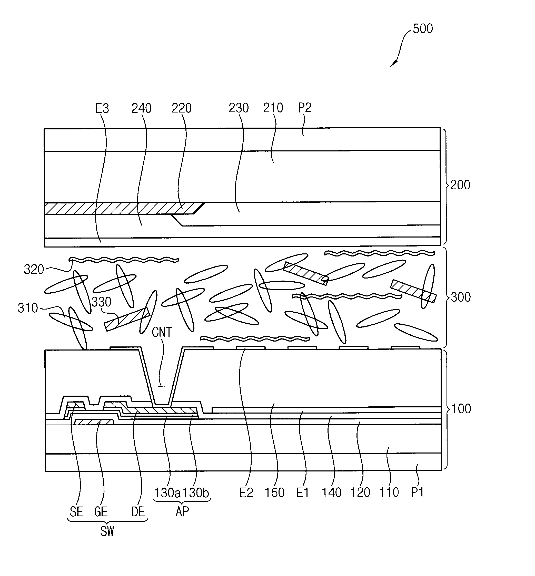
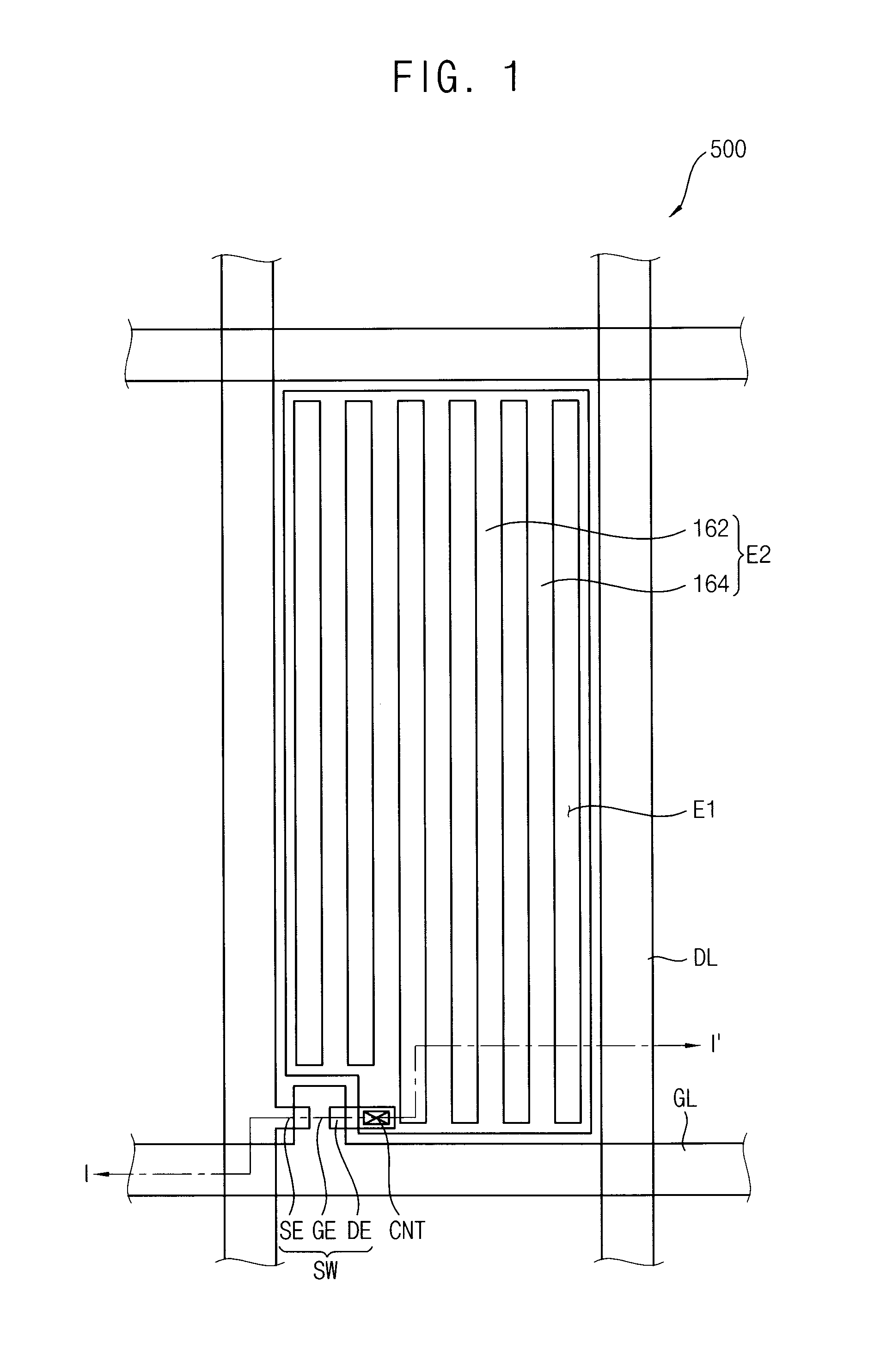
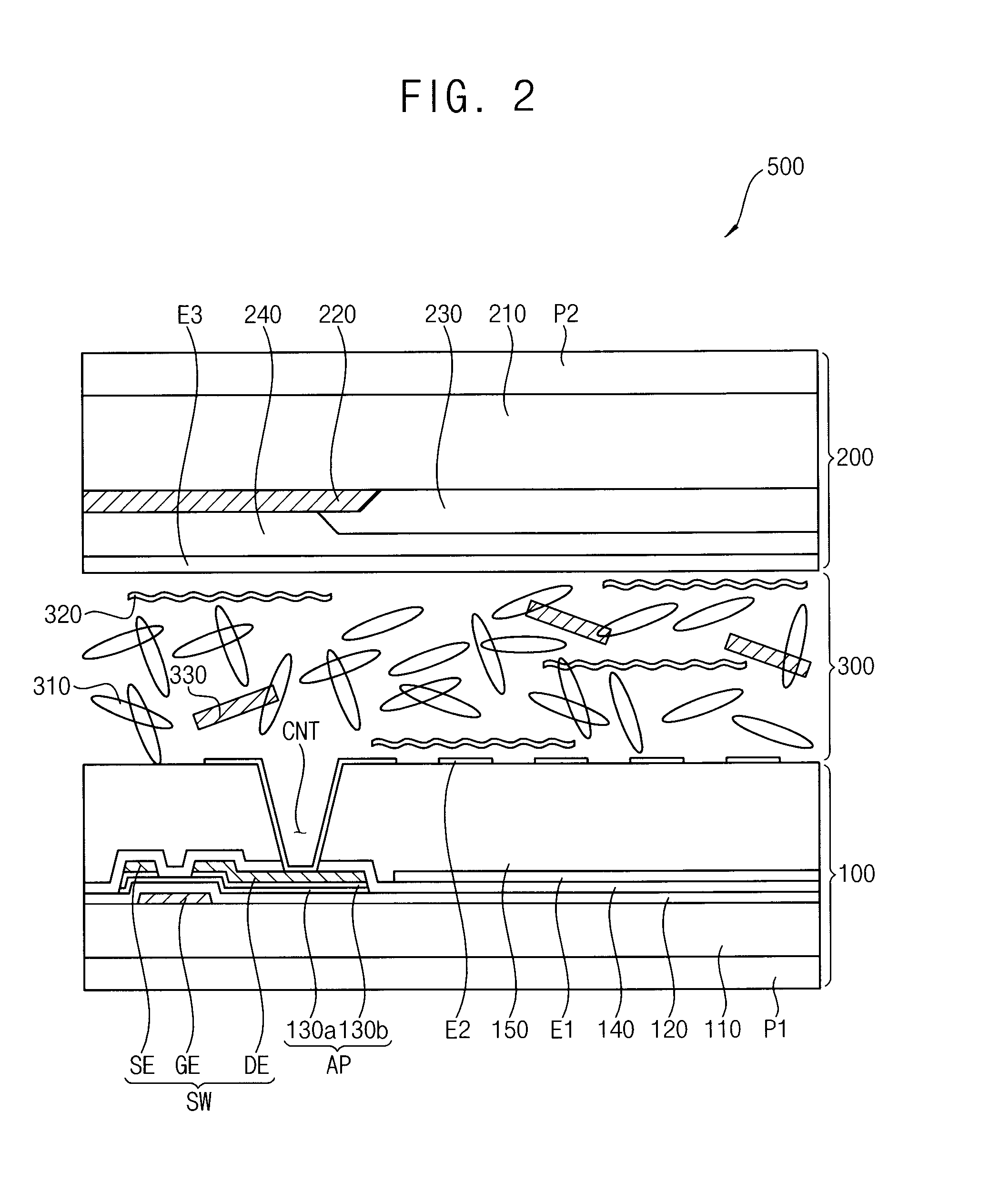
[0026]The invention is described more fully hereinafter with reference to the accompanying drawings, in which embodiments of the invention are shown. This invention may, however, be embodied in many different forms and should not be construed as limited to the embodiments set forth herein. Rather, these embodiments are provided so that this disclosure is thorough, and will fully convey the scope of the invention to those skilled in the art. In the drawings, the size and relative sizes of layers and regions may be exaggerated for clarity Like reference numerals in the drawings denote like elements.

[0027]It will be understood that when an element or layer is referred to as being “on” or “connected to” another element or layer, it can be directly on or directly connected to the other element or layer, or intervening elements or layers may be present. In contrast, when an element or layer is referred to as being “directly on” or “directly connected to” another element or layer, there ar...


PUM


Abstract

In a display panel and a method of manufacturing the display panel, the display panel includes a display substrate including a first electrode and a second electrode insulated from the first electrode and disposed on the first electrode, an opposite substrate including a third electrode facing the second electrode, and a liquid crystal layer interposed between the display substrate and the opposite substrate. The liquid crystal layer includes liquid crystal molecules, a reactive mesogen polymer, and nano-rods.

Description

CROSS REFERENCE TO RELATED APPLICATION[0001]This application claims priority from and the benefit of Korean Patent Application No. 2011-0095999, filed on Sep. 23, 2011, which is hereby incorporated by reference for all purposes as if fully set forth herein.BACKGROUND OF THE INVENTION[0002]1. Field of the Invention[0003]Exemplary embodiments of the present invention relate to a display panel and a method of manufacturing the display panel. Exemplary embodiments of the present invention relate to a display panel used for a liquid crystal display apparatus and a method of manufacturing the display panel.[0004]2. Discussion of the Background[0005]Generally, a display panel includes a display substrate including a switching element for driving a pixel, an opposite substrate facing the display substrate, and a liquid crystal layer interposed between the display substrate and the opposite substrate. When an electric field is formed in the liquid crystal layer, an alignment of liquid crysta...

Claims


Application Information

Patent Timeline
IPC IPC(8): C09K19/54C09K19/52G02F1/1343H01J9/20B82B1/00B82Y20/00
CPCB82Y20/00C09K19/52G02F2001/134381C09K2019/0448C09K2019/528G02F1/1343G02F1/134381C09K19/00G02F1/13G02F1/1337G02F1/13439G02F1/1368G02F1/134363
Inventor RHO, SOON-JOONLEE, HYEOK-JINBAE, JI-HONGPARK, JUN-HAJANG, HYE-LIMYOON, TAE-HOONSONG, DONG-HANKIM, KI-HANKIM, JUNG-WOOK
Owner SAMSUNG DISPLAY CO LTD
Why Eureka
Try Eureka