Multi-gate field-effect transistors with variable fin heights

a field-effect transistor and variable fin height technology, applied in the field of multi-gate field-effect transistor devices, can solve the problems of increasing power consumption in idle state of effect transistor devices, finding to be increasingly inefficient on the nanometer scale,

Inactive Publication Date: 2013-04-04
GLOBALFOUNDRIES INC
View PDF8 Cites 32 Cited by
  • Summary
  • Abstract
  • Description
  • Claims
  • Application Information

AI Technical Summary

Benefits of technology

[0009]Another embodiment is directed to a method for fabricating a circuit apparatus. In accordance with the method, at least one recess is formed in a substrate that is composed of a semiconducting material such that a difference between a depth of the at least one recess and a height of a surface of the substrate effects differences in height between fins of a plurality of fins. In addition, the substrate is etched to form the plurality of fins, wherein a first fin of the plurality of fins has a first height that is different fr

Problems solved by technology

Planar field-effect transistor (FET) devices, which have been widely used in integrated circuits for the past several decades, were found to be increasingly inefficient on the nanometer scale.
Reducing the size of

Method used


Image

  • Multi-gate field-effect transistors with variable fin heights
  • Multi-gate field-effect transistors with variable fin heights
  • Multi-gate field-effect transistors with variable fin heights

Examples


Embodiment Construction

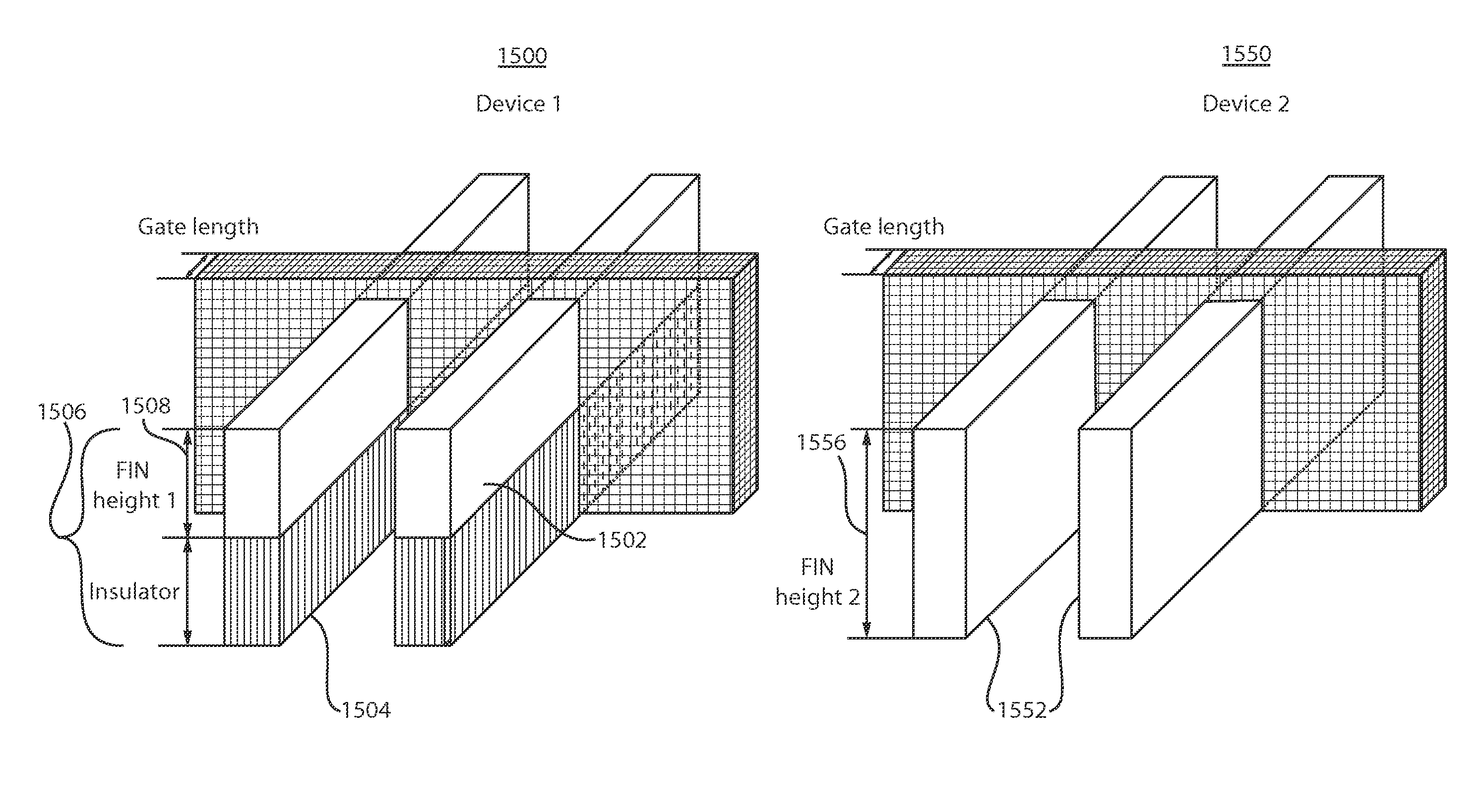
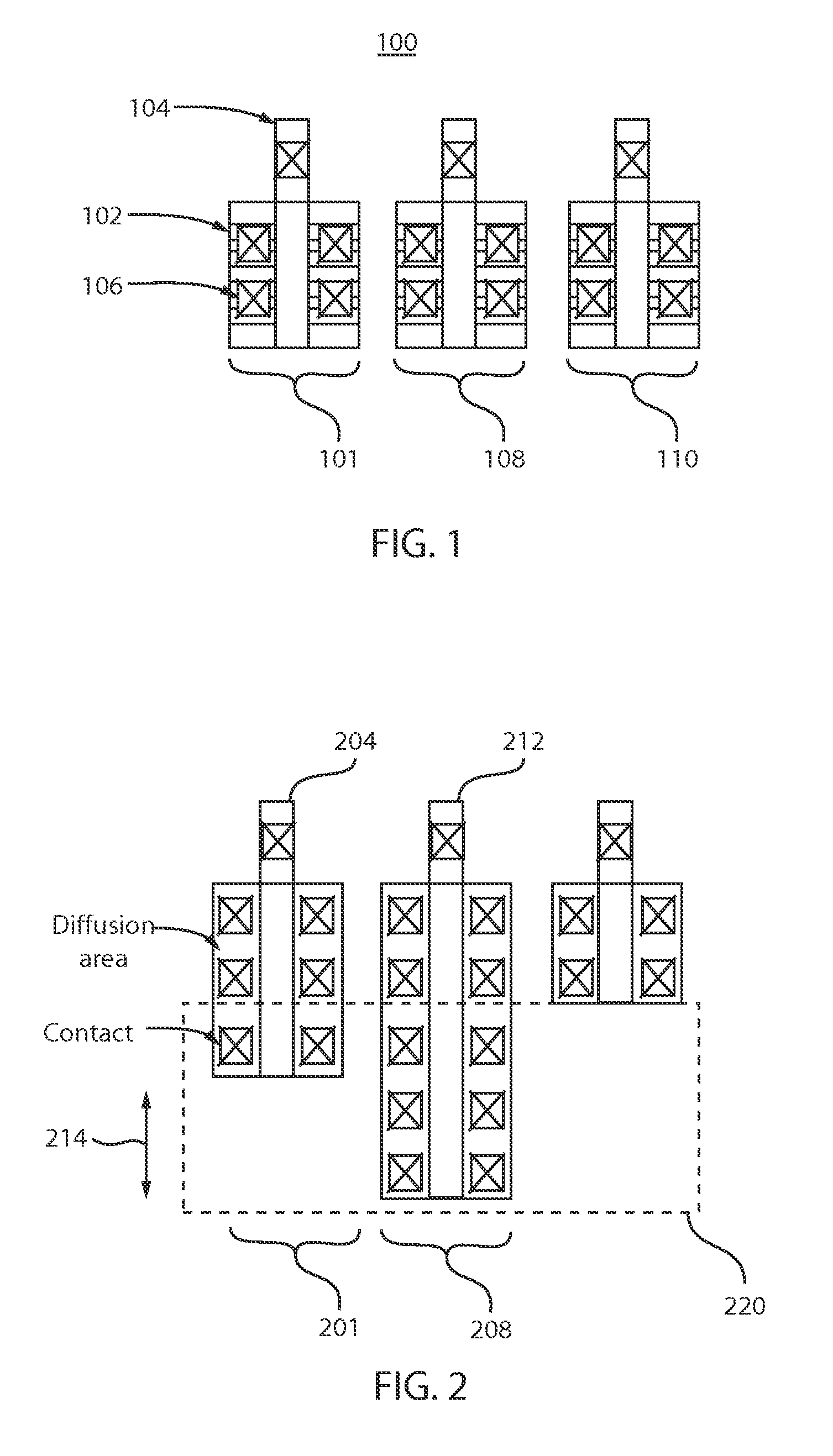
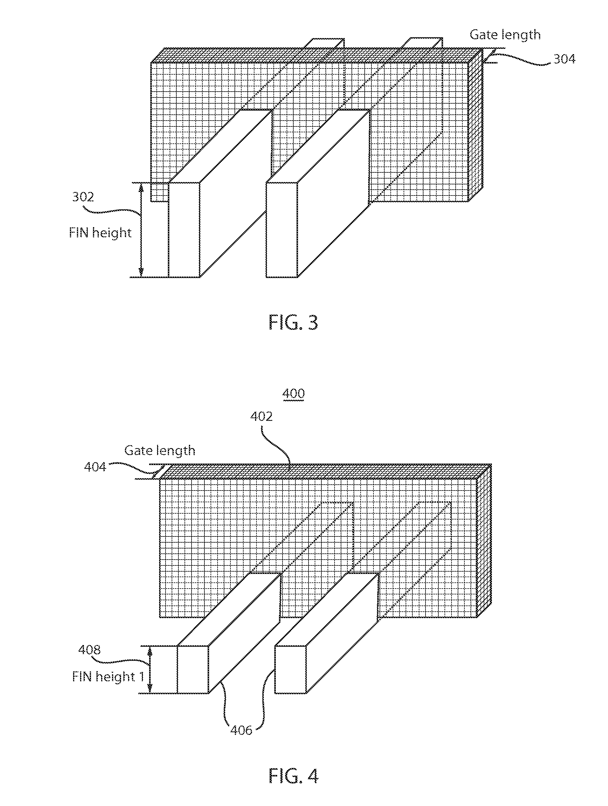
[0028]In addition to the benefit of suppressing leakage current described above, another advantage of multi-gate devices is that the drive current of the devices can be altered without affecting the layout area occupied by the device on an integrated circuit. For example, referring now to the drawings in which like numerals represent the same or similar elements and initially to FIG. 1, a first implementation 100 of a circuit including FinFET devices is illustrated. Each of the devices 101 includes fins 102, a gate 104 and contacts 106. Assume that it is desirable for the drive current for two of the FinFET devices to be modified. The drive current is an important design parameter, as an improper drive current can damage elements of a circuit. The traditional means of controlling the drive current, as in planar devices, is to adjust the width of the gate. For example, referring to FIG. 2, with continuing reference to FIG. 1, the widths of the gates of device 101 and 108 can be exten...


PUM


Abstract

Multi-gate devices and methods of their fabrication are disclosed. A multi-gate device can include a gate structure and a plurality of fins. The gate structure envelops a plurality of surfaces of the fins, which are directly on a substrate that is composed of a semiconducting material. Each of the fins provides a channel between a respective source and a respective drain, is composed of the semiconducting material and is doped. A first fin of the plurality of fins has a first height that is different from a second height of a second fin of the plurality of fins such that drive currents of the first and second fins are different. Further, the first and second fins form a respective cohesive structure of the semiconducting material with the substrate. In addition, surfaces of the substrate that border the fins are disposed at a same vertical position.

Description

RELATED APPLICATION DATA[0001]This application is a Continuation application of co-pending U.S. patent application Ser. No. 13 / 251,815 filed on Oct. 3, 2011, incorporated herein by reference in its entirety.BACKGROUND[0002]1. Technical Field[0003]The present invention relates to semiconductor devices, and more particularly, to multi-gate field-effect transistor devices and fabrication methods.[0004]2. Description of the Related Art[0005]Throughout the evolution and advancement of computing devices, reducing their size and their power consumption while maintaining or improving a high processing capacity have long been design goals. Planar field-effect transistor (FET) devices, which have been widely used in integrated circuits for the past several decades, were found to be increasingly inefficient on the nanometer scale. Reducing the size of the channel between the terminals of planar transistors to this scale leads to an inefficient leakage of current in the off-state of the transis...

Claims


Application Information

Patent Timeline
IPC IPC(8): H01L27/088
CPCH01L27/0886H01L21/823431
Inventor CHEN, HSUEH-CHUNGFAN, SU CHENSTANDAERT, THEODORUS E.YEH, CHUN-CHEN
Owner GLOBALFOUNDRIES INC
Why Eureka
Try Eureka