Logical to physical address mapping in storage systems comprising solid state memory devices

a storage system and physical address technology, applied in the direction of memory adressing/allocation/relocation, instruments, computing, etc., can solve the problem that the main memory size goes beyond the economic efficiency

Active Publication Date: 2013-05-16
IBM CORP
View PDF22 Cites 94 Cited by
  • Summary
  • Abstract
  • Description
  • Claims
  • Application Information

AI Technical Summary

Problems solved by technology

However, with an increase in flash memory capacity, the address mapping information also increases to a level where the entire mapping information will cause the main memory size go beyond economic efficiency.
However, depending on the state of CMT and the replacement algorithm being used, it may entail evicting entries from SRAM.

Method used


Image

  • Logical to physical address mapping in storage systems comprising solid state memory devices
  • Logical to physical address mapping in storage systems comprising solid state memory devices
  • Logical to physical address mapping in storage systems comprising solid state memory devices

Examples


Embodiment Construction

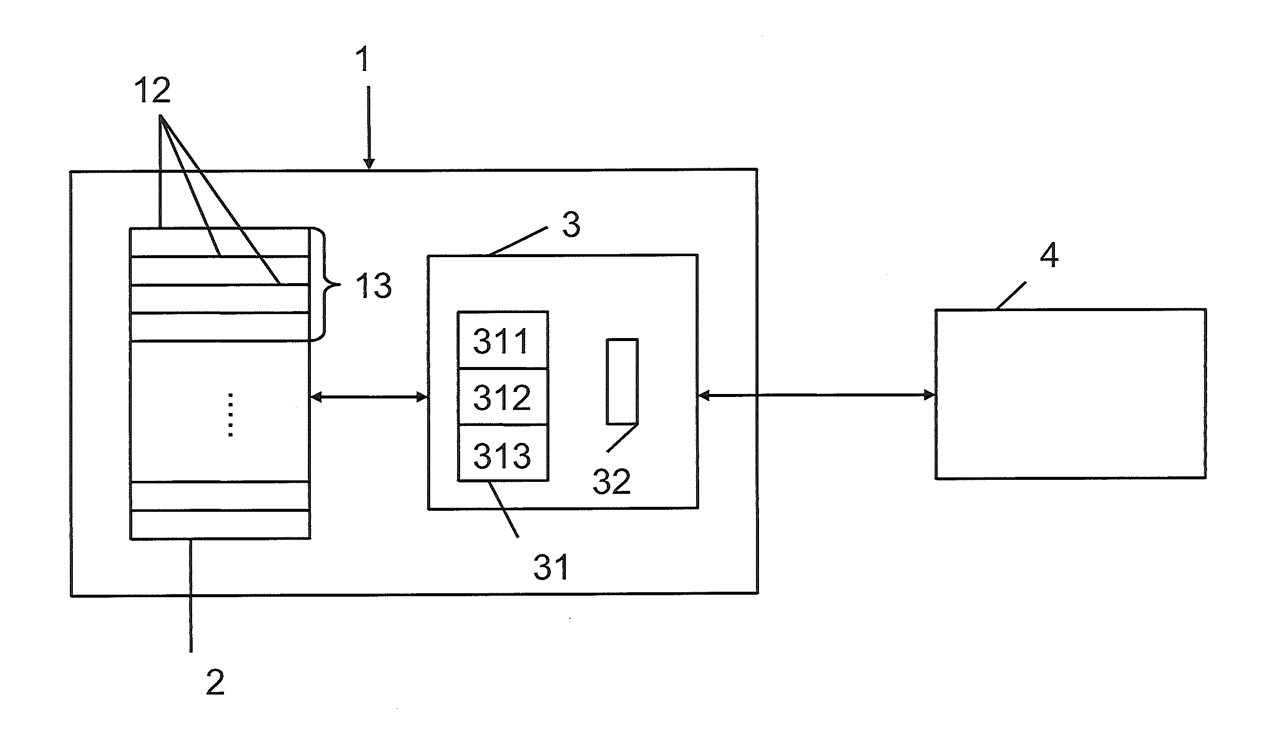
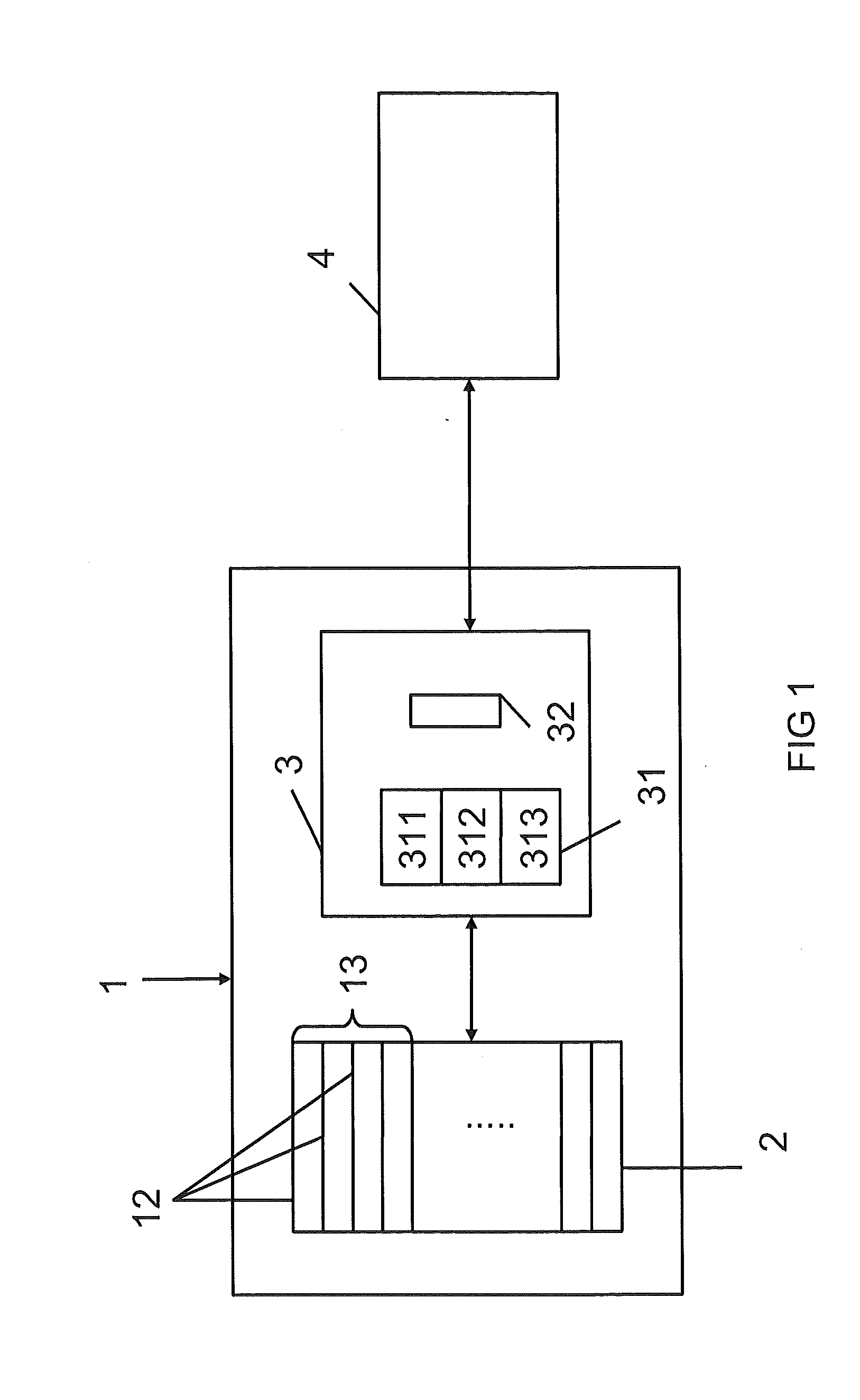
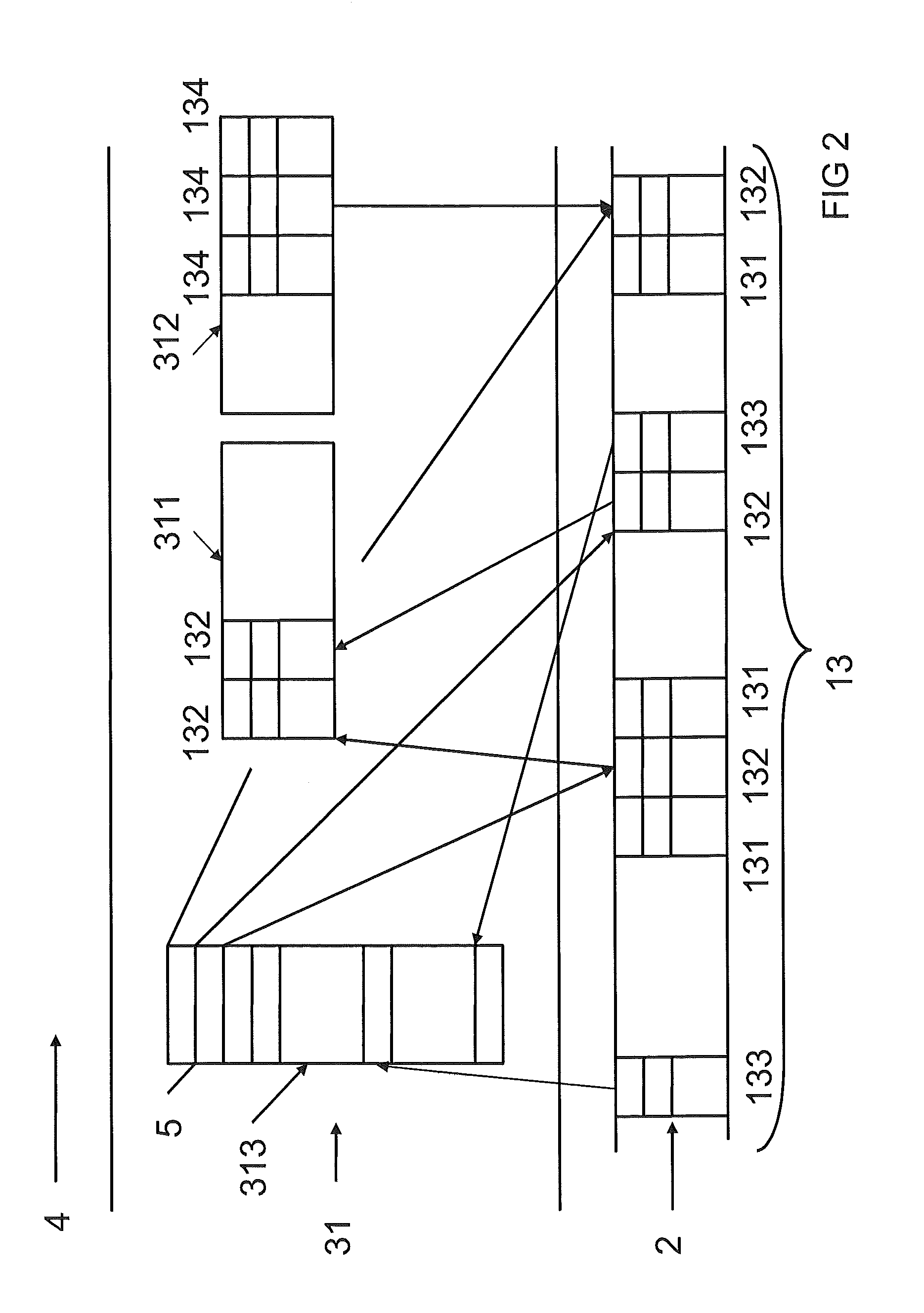
[0039]As an introduction to the following description, it is first pointed at a general aspect of the invention, concerning a storage controller for controlling reading and writing of data from / to a solid state memory device. There is provided a read cache for buffering address mapping information representing a subset of address mapping information stored in the memory device. The address mapping information includes a mapping of logical address information for identifying data in a requesting host to physical address information for identifying data in the memory device. In addition to the read cache, a dedicated write cache is provided for buffering address mapping information to be written to the memory device. In other words, the present concept is applicable even to solid state memory devices with huge capacity for the reason that the complete address mapping information will be stored in the solid state memory device itself. Only portions of it—which portions are collectively...


PUM


Abstract

The present idea provides a high read and write performance from / to a solid state memory device. The main memory of the controller is not blocked by a complete address mapping table covering the entire memory device. Instead such table is stored in the memory device itself, and only selected portions of address mapping information are buffered in the main memory in a read cache and a write cache. A separation of the read cache from the write cache enables an address mapping entry being evictable from the read cache without the need to update the related flash memory page storing such entry in the flash memory device. By this design, the read cache may advantageously be stored on a DRAM even without power down protection, while the write cache may preferably be implemented in nonvolatile or other fail-safe memory. This leads to a reduction of the overall provisioning of nonvolatile or fail-safe memory and to an improved scalability and performance.

Description

PRIORITY[0001]This is a U.S. national stage of application No.: PCT / IB2011 / 053299, filed Jul. 25, 2011. Priority under 35 U.S.C. §119(a) and 35 U.S.C. §365(b) is claimed from European Patent Application No. 10170863.4, filed Jul. 27, 2010, and all the benefits accruing therefrom under 35 U.S.C. §119, the contents of which in its entirety are herein incorporated by reference.FIELD OF THE INVENTION[0002]The present invention generally relates to storage systems comprising solid state memory devices such as flash based memory devices, and to techniques for efficiently providing read and / or write access to data stored on such memory devices, in particular with a focus on logical to physical address mapping.BACKGROUND[0003]Solid-state memory devices encompass rewritable non-volatile memory devices which use electronic circuitry for storing data. Currently, solid-state memory devices start replacing conventional storage devices such as hard disk drives and optical disk drives in some aren...

Claims


Application Information

Patent Timeline
Patent Type & Authority Applications(United States)
IPC IPC(8): G06F12/02G06F12/0846G06F12/0866G06F12/0886
CPCG06F12/0246G06F12/0848G06F12/0866G06F2212/7201G06F2212/221G06F2212/222G06F2212/466G06F2212/214G06F12/0886
Inventor BUX, WERNERHAAS, ROBERTHU, XIAO-YUPLETKA, ROMAN
Owner IBM CORP
Why Eureka
Try Eureka