Illumination device

a technology of illumination device and organic electroluminescence device, which is applied in the direction of thermoelectric devices, organic semiconductor devices, solid-state devices, etc., can solve the problems of difficult to fabricate a desirable large-scale organic electroluminescence device for lighting applications, and the light emitting uniformity of the organic electroluminescence device is usually deteriorated, so as to achieve the effect of desirable light emitting efficiency

Inactive Publication Date: 2013-06-13
AU OPTRONICS CORP
View PDF5 Cites 10 Cited by
  • Summary
  • Abstract
  • Description
  • Claims
  • Application Information

AI Technical Summary

Benefits of technology

[0007]In one aspect is directed to an illumination device having uniformed light emitting effect and desirable light emitting efficiency.

Problems solved by technology

However, the light emitting uniformity of the organic electroluminescence device is usually deteriorated with the increasing of the size.
Therefore, it is still difficult to fabricate a desirable large sized organic electroluminescence device for the lighting application.

Method used


Image

  • Illumination device
  • Illumination device
  • Illumination device

Examples


Embodiment Construction

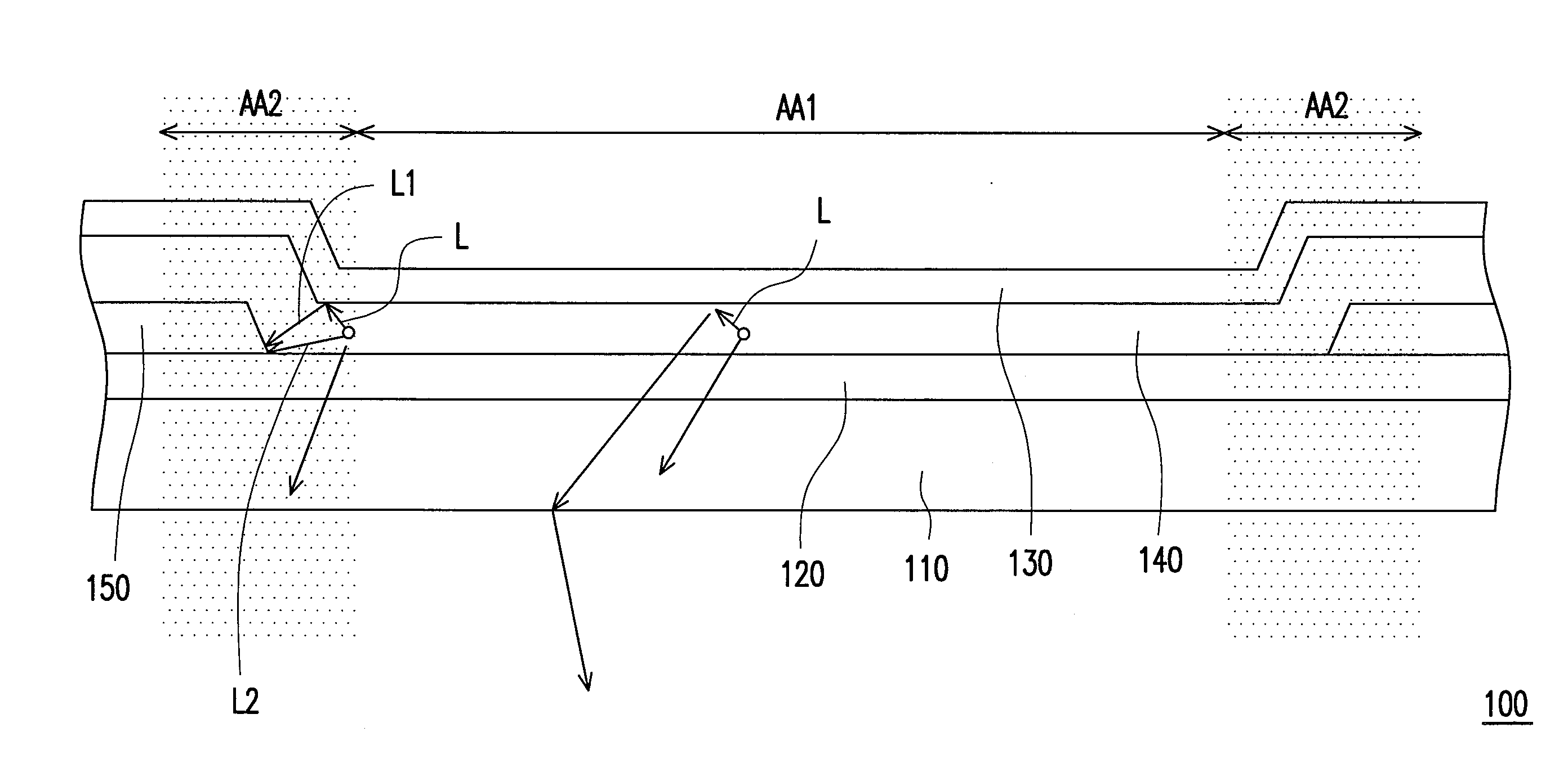
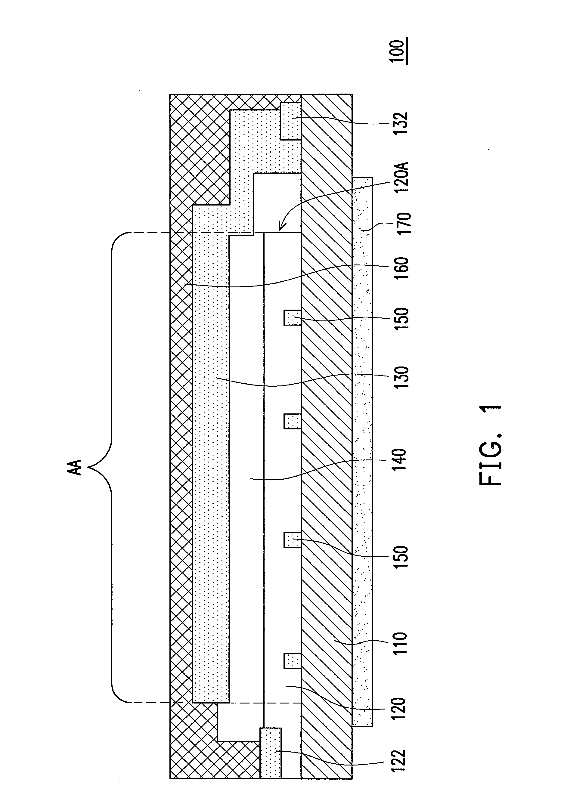
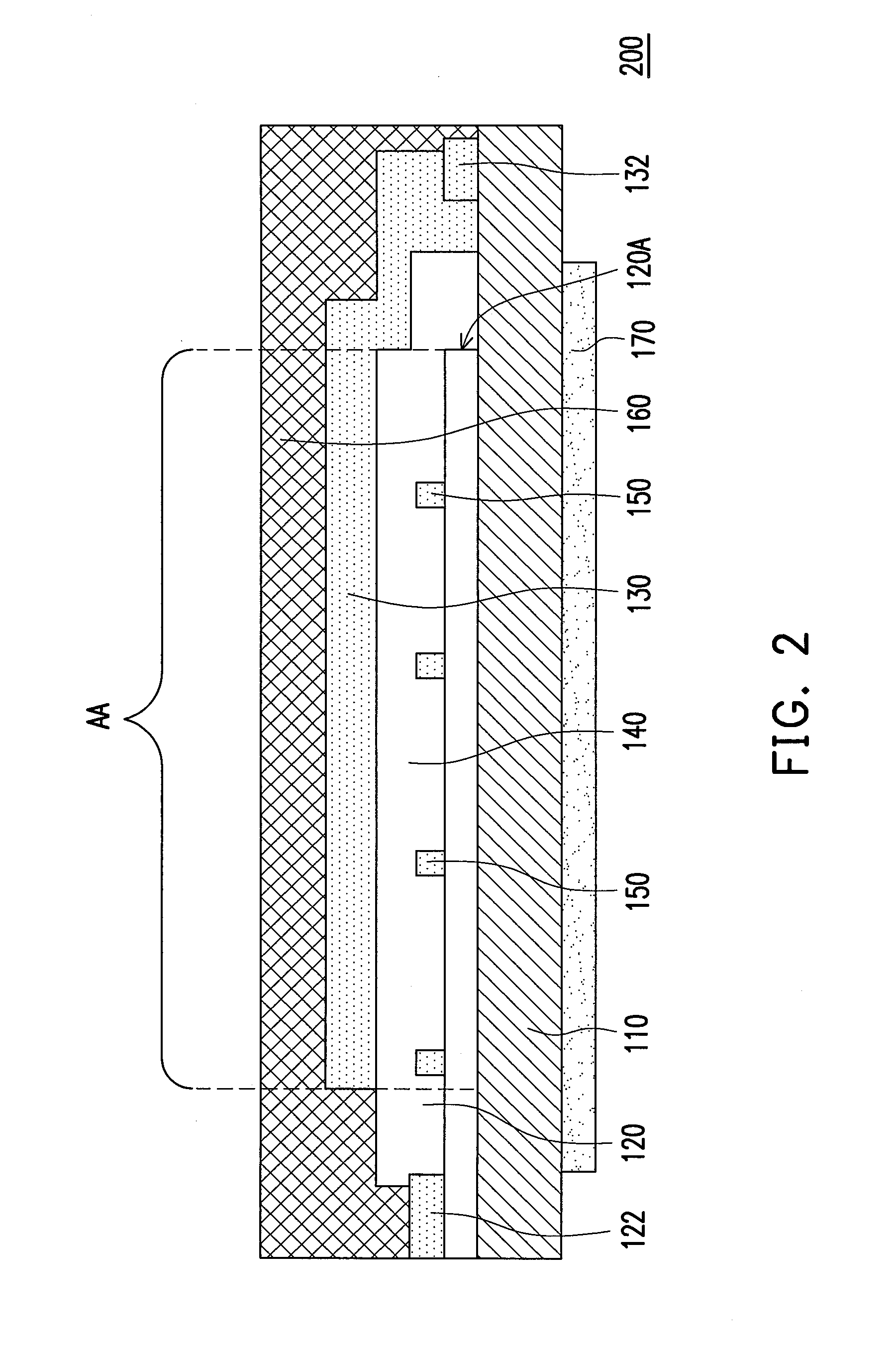
[0027]FIG. 1 through FIG. 5 is respectively a schematic cross-sectional view illustrating an illumination device according to an exemplary embodiment. Referring to FIG. 1, an illumination device 100 includes a substrate 110, a first conductive layer 120, a second conductive layer 130, a self-illuminating layer 140, a first auxiliary conductive pattern layer 150, a protection material 160, and a light extraction layer 170. The first conductive layer 120, the second conductive layer 130, the self-illuminating layer 140, the first auxiliary conductive pattern layer 150, the protection material 160, and the light extraction layer 170 are disposed on the substrate 110.

[0028]The first conductive layer 120, the second conductive layer 130, and the self-illuminating layer 140 are stacked on a same side of the substrate 110 which is the first surface of the substrate 110 (or namely the inner surface of the substrate 110) and the self-illuminating layer 140 is disposed between the first condu...


PUM


Abstract

An illumination device including a substrate, a first conductive layer, a second conductive layer, a self-illuminating layer, and a first auxiliary conductive pattern layer is provided. The first conductive layer and the second conductive layer are disposed on the substrate. The self-illuminating layer is located between the first conductive layer and the second conductive layer to define an illumination region on the substrate. The first auxiliary conductive pattern layer is in contact with the first conductive layer and has an impedance smaller than that of the first conductive layer. A ratio of a perimeter (um) of the first auxiliary conductive pattern layer occupied in the illumination region to an area (um2) of the illumination region is greater than about 0 and smaller than or equal to about 0.0262 (1/um).

Description

CROSS-REFERENCE TO RELATED APPLICATION[0001]This application claims the priority benefit of Taiwan application serial no. 100145077, filed on Dec. 7, 2011. The entirety of the above-mentioned patent application is hereby incorporated by reference herein and made a part of this specification.BACKGROUND OF THE DISCLOSURE[0002]1. Field of the Invention[0003]The document relates to an illumination device, and particularly to a self-illuminating type illumination device.[0004]2. Description of Related Art[0005]Organic electroluminescent devices have been considered a dominant flat panel display in the future because of their desirable qualities of compactness, self-luminescence, low power consumption, no need of backlight source, no viewing angle limitation, and high response speed. In addition, a passive organic electroluminescent device can be fabricated on a thin, light, and flexible substrate so as to be suitable for the lighting application. Generally, if the light emitting efficien...

Claims


Application Information

Patent Timeline
Patent Type & Authority Applications(United States)
IPC IPC(8): H01L51/52
CPCH01L51/5212H01L2251/5361H01L51/5228H10K50/814H10K50/824
Inventor LIN, CHEN-CHICHIANG, PO-HSUANWU, CHANG-YENLIN, CHUN-LIANG
Owner AU OPTRONICS CORP
Why Eureka
Try Eureka