Semiconductor device and method for manufacturing the same

Inactive Publication Date: 2013-06-13
SK HYNIX INC
View PDF3 Cites 188 Cited by
  • Summary
  • Abstract
  • Description
  • Claims
  • Application Information

AI Technical Summary

Benefits of technology

[0027]An embodiment of the present invention relates to a semiconductor device and a method for manufacturing the same, in which a first end of a fuse line is coupled to a lower end, a second end located opposite to the first end of the fuse line is coupled to an upper line, and a fuse blowing region is formed at one

Problems solved by technology

As a result, defective cells may be detected by the EDS process in early stages of manufacture and repaired.
As a result, an explosion occurs and the fuse is blown.
However, when the insulation film is thick, a crack occurs in a lower part of the insulation film prior to execution of the explosion, and a metal permeates into the crack, causing an unwanted short circuit.
Thus, it becomes dif

Method used


Image

  • Semiconductor device and method for manufacturing the same
  • Semiconductor device and method for manufacturing the same
  • Semiconductor device and method for manufacturing the same

Examples


Embodiment Construction

[0046]Reference will now be made in detail to embodiments of the present invention, examples of which are illustrated in the accompanying drawings. Wherever possible, the same reference numbers will be used throughout the drawings to refer to the same or like parts.

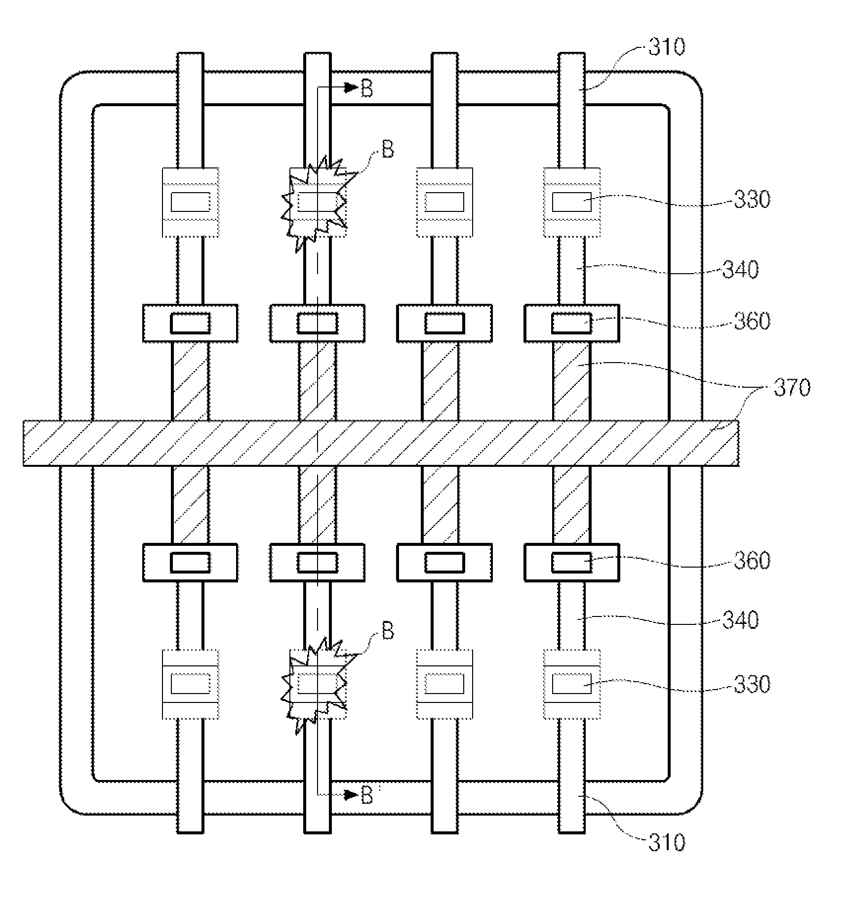
[0047]FIG. 3 is a plan view illustrating a semiconductor device manufactured by a method according to an embodiment of the present invention. FIG. 4 is a cross-sectional view of the semiconductor device taken along the line B-B′ of FIG. 3.

[0048]Referring to FIGS. 3 and 4, the semiconductor device includes a semiconductor substrate 300, a first line pattern 310, a first contact plug 330, a fuse pattern 340, a second contact plug 330, a fuse pattern 340, a second contact plug 360, and a second line pattern 370.

[0049]According to an embodiment of the present invention, the first line pattern 310 is formed over the semiconductor substrate 300, and the first contact plug 330 is coupled to one end of the first line pattern 310....


PUM


Abstract

A semiconductor device includes: a fuse pattern formed at a first level, a first line pattern formed at a second level lower than the first level, a second line pattern formed at a third level higher than the first level, a first contact plug coupling the fuse pattern to the first line pattern 310, a second contact plug coupling the fuse pattern to the second line pattern, and a fuse blowing region provided over first line pattern and overlapping with the first contact plug at least partially.

Description

CROSS-REFERENCE TO RELATED APPLICATION[0001]The priority of Korean patent application No. 10-2011-0130829 filed on 8 Dec. 2011, the disclosure of which is hereby incorporated in its entirety by reference, is claimed.BACKGROUND OF THE INVENTION[0002]Embodiments of the present invention relate to a semiconductor device and a method for manufacturing the same, and more particularly, to a semiconductor device including a fuse and a method of manufacturing the same.[0003]In recent times, as information media such as computers have rapidly come into widespread use, technology of a semiconductor device has been rapidly developed. Functionally, it is necessary for a semiconductor device to operate at a high speed and to have a high storage capacity. Therefore, technology for manufacturing semiconductor devices has rapidly developed to improve integration degree, reliability, response speed, etc.[0004]A process for manufacturing semiconductor devices includes a fabrication (FAB) process that...

Claims


Application Information

Patent Timeline
IPC IPC(8): H01L23/525H01L21/768
CPCH01L23/5256H01L21/76886H01L2924/0002H01L23/5258H01L2924/00H01L21/82
Inventor KIM, DONG HOON
Owner SK HYNIX INC
Why Eureka
Try Eureka