Array substrate and liquid crystal display panel

Active Publication Date: 2013-06-27
BOE TECH GRP CO LTD
View PDF4 Cites 1 Cited by
  • Summary
  • Abstract
  • Description
  • Claims
  • Application Information

AI Technical Summary

Problems solved by technology

In the prior art, because the first electrode in an AD-SDS type array substrate is a planar structure without apertures, the overlapping area between the second electrode and the first electrod

Method used


Image

  • Array substrate and liquid crystal display panel
  • Array substrate and liquid crystal display panel
  • Array substrate and liquid crystal display panel

Examples


Embodiment Construction

[0014]In order to make objects, technical details and advantages of the embodiments of the invention apparent, the technical solution of the embodiment will be described in a clearly and fully understandable way in connection with the drawings related to the embodiments of the invention. It is obvious that the described embodiments are just a part but not all of the embodiments of the invention. Based on the described embodiments herein, those skilled in the art can obtain other embodiment(s), without any inventive work, which should be within the scope of the invention.

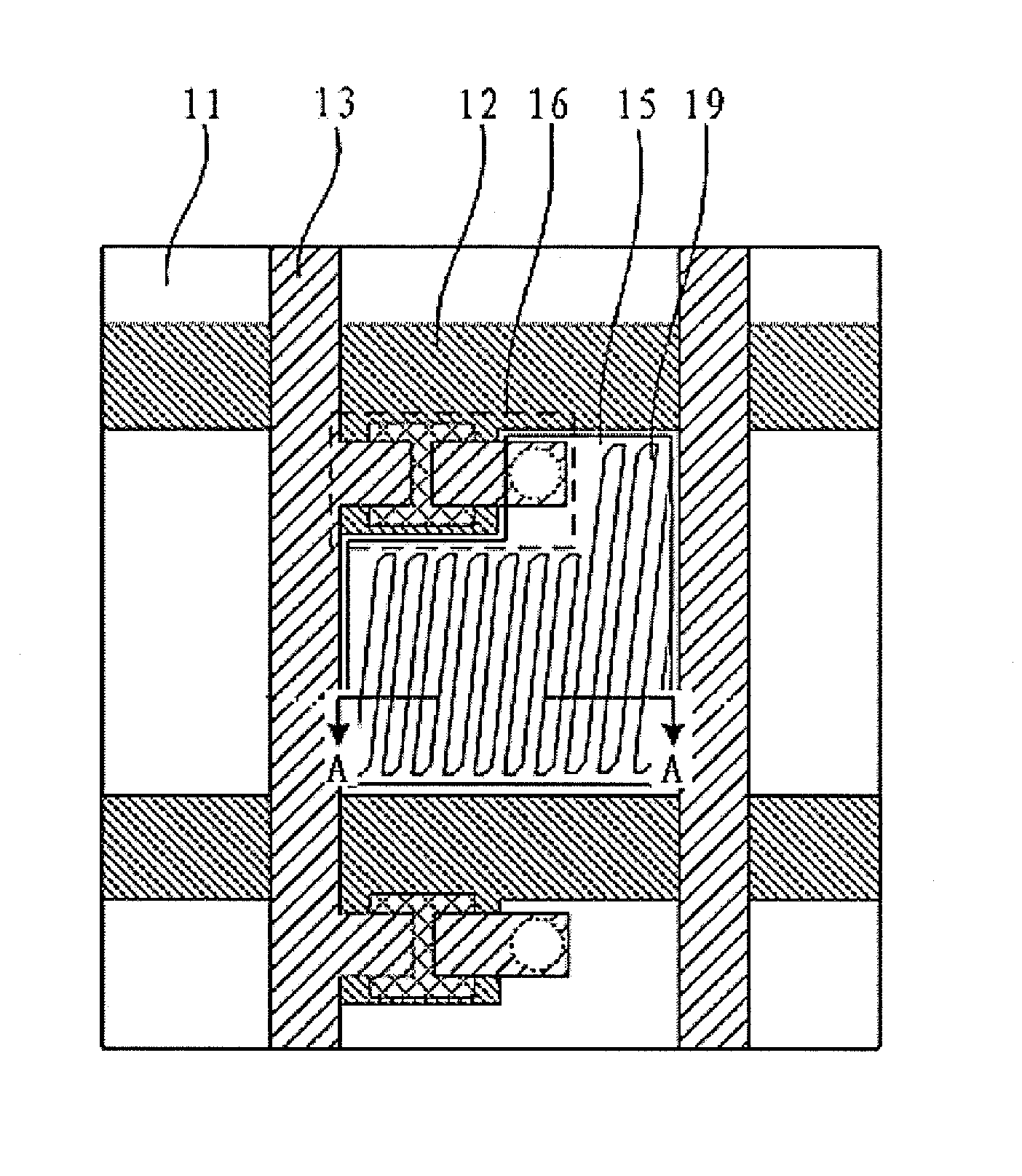
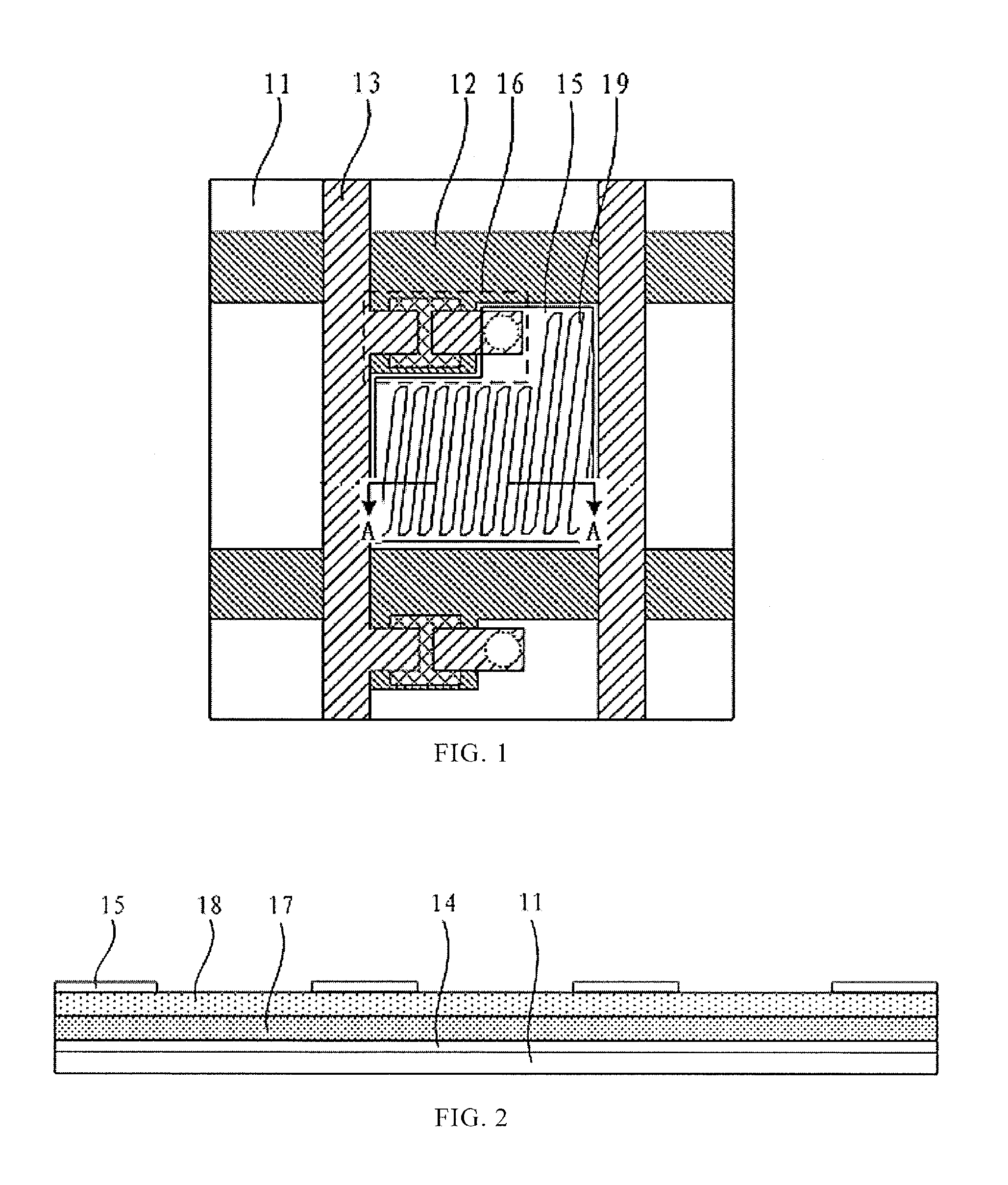
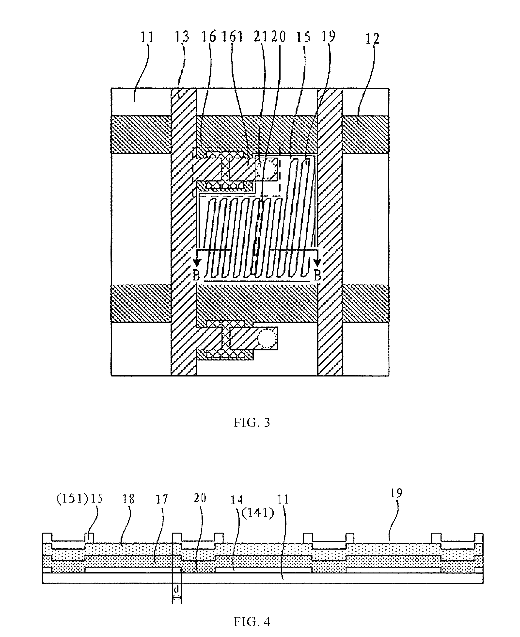
[0015]FIG. 3 is a schematic structural view of an array substrate provided by a first embodiment of the disclosed technical solution, and FIG. 4 is a sectional view taken along the B-B direction in FIG. 3. As shown in FIG. 3 and FIG. 4, the array substrate comprises: a base substrate 11, as well as a gate line 12 and a data line 13 formed on the base substrate 11. The gate line 12 and the data line 13 cross with each...


PUM


Abstract

The disclosed technology discloses an array substrate and a liquid crystal display panel. The array substrate comprises: a base substrate; a gate line and a data line formed on the base substrate, the gate line and the data line defining a plurality of pixel regions; and a first electrode layer and a second electrode layer formed in each pixel region; and an insulating layer provided between the first electrode layer and the second electrode layer. The first electrode layer, the insulating layer and the second electrode layer are laminated on the base substrate in this order. The first electrode layer is provided with a plurality of first apertures therein, and the first electrode layer comprises a plurality of first electrode portions located between the plurality of first apertures.

Description

FIELD OF THE INVENTION[0001]The disclosed technology relates to an array substrate and a liquid crystal display panel.BACKGROUND OF THE INVENTION[0002]An Advanced-Super Dimensional Switching (AD-SDS) technology, by forming a multi-dimensional electric field with a transversal electric field generated from edges of common electrodes or pixel electrodes in the same plane and a longitudinal electric field generated between the pixel electrodes and the common electrodes, enables liquid crystal molecules in all orientations between the pixel electrodes or common electrodes as well as right above the pixel electrodes or common electrodes within a liquid crystal cell to produce rotation switching, and thus improves work efficiency of an in-plane alignment liquid crystal and increases light transmission efficiency. The Advanced-Super Dimensional Switching technology can improve display quality of a TFT-LCD, and has advantages of high transmittance, wide viewing angle, high aperture ratio, l...

Claims


Application Information

Patent Timeline
IPC IPC(8): H01L33/08G02F1/1343
CPCG02F1/134309G02F2001/134318G02F1/134363H01L33/08G02F1/134318
Inventor MA, XINLILI, YANWANG, QIANGTAOLI, WENBING
Owner BOE TECH GRP CO LTD
Why Eureka
Try Eureka