Semiconductor Package with a Bridge Interposer

a technology of interposer and semiconductor, applied in the direction of semiconductor device, semiconductor/solid-state device details, electrical apparatus, etc., can solve the problem of adversely affecting the electrical signal passing through the conventional interposer

Active Publication Date: 2013-07-04
AVAGO TECH INT SALES PTE LTD
View PDF6 Cites 128 Cited by
  • Summary
  • Abstract
  • Description
  • Claims
  • Application Information

AI Technical Summary

Problems solved by technology

However, leakage through the semiconductor substrate resulting from parasitic coupling amongst the TSVs can adversely affect electrical signals passing through conventional interposers.

Method used


Image

  • Semiconductor Package with a Bridge Interposer
  • Semiconductor Package with a Bridge Interposer
  • Semiconductor Package with a Bridge Interposer

Examples


Embodiment Construction

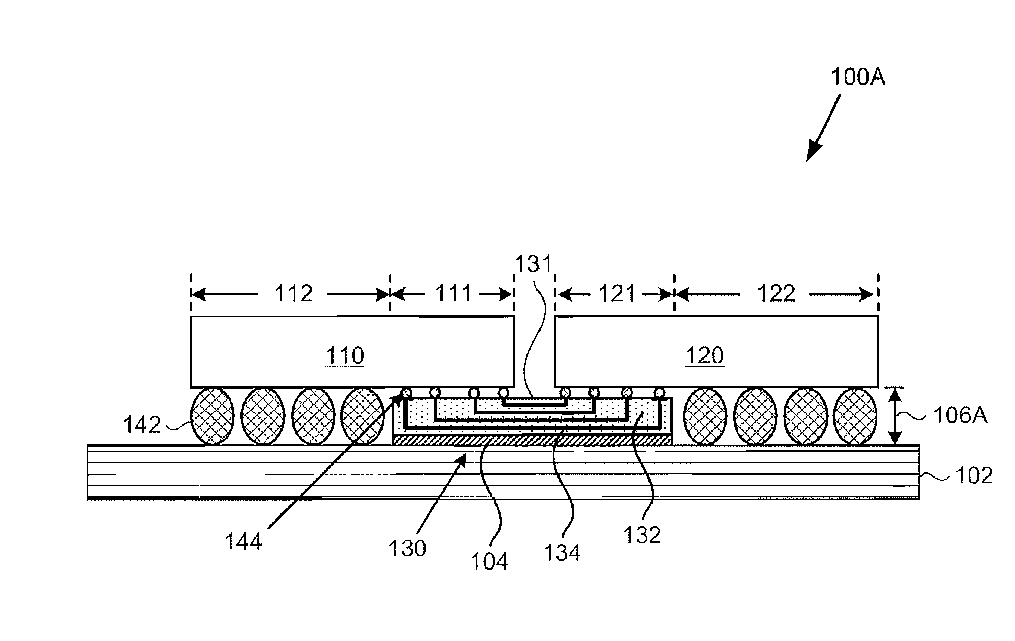
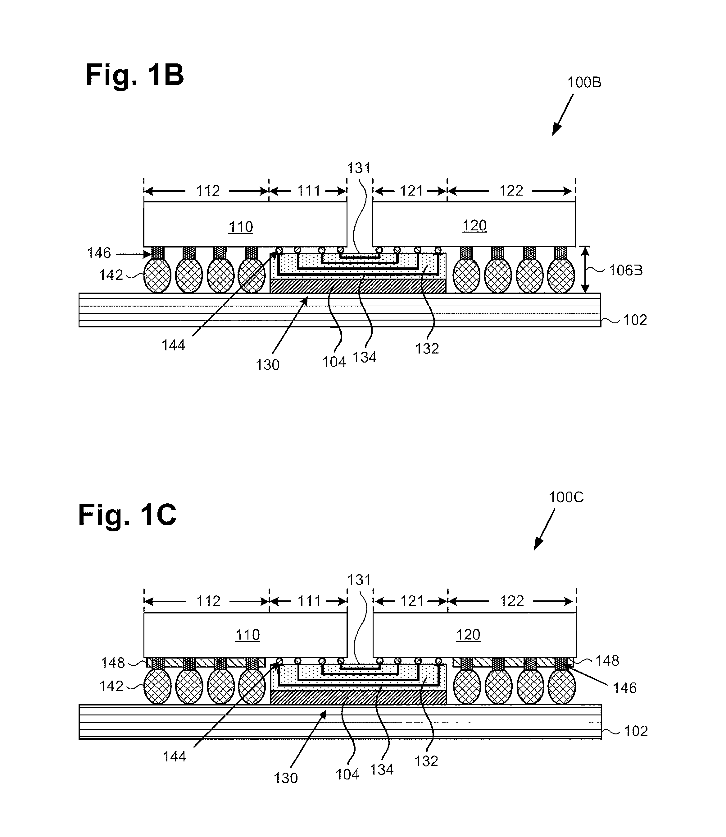
[0009]The following description contains specific information pertaining to implementations in the present disclosure. One skilled in the art will recognize that the present disclosure may be implemented in a manner different from that specifically discussed herein. The drawings in the present application and their accompanying detailed description are directed to merely exemplary implementations. Unless noted otherwise, like or corresponding elements among the figures may be indicated by like or corresponding reference numerals. Moreover, the drawings and illustrations in the present application are generally not to scale, and are not intended to correspond to actual relative dimensions.

[0010]FIG. 1A shows a cross-sectional view of one implementation of a semiconductor package including a bridge interposer. As shown in FIG. 1A, semiconductor package 100A includes first active die 110 having first portion 111 and second portion 112, second active die 120 having first portion 121 and...


PUM


Abstract

There are disclosed herein various implementations of semiconductor packages including a bridge interposer. One exemplary implementation includes a first active die having a first portion situated over the bridge interposer, and a second portion not situated over the bridge interposer. The semiconductor package also includes a second active die having a first portion situated over the bridge interposer, and a second portion not situated over the bridge interposer. The second portion of the first active die and the second portion of the second active die include solder balls mounted on a package substrate, and are configured to communicate electrical signals to the package substrate utilizing the solder balls and without utilizing through-semiconductor vias (TSVs).

Description

BACKGROUND[0001]Packaging solutions continue to evolve to meet the increasingly stringent design constraints imposed by electronic devices and systems with ever higher integrated circuit (IC) densities. One solution for providing power and ground connections, as well as input / output (I / O) signals, for example, to multiple active dies within a single semiconductor package utilizes one or more interposers to electrically couple the active dies to the package substrate.[0002]A conventional interposer implemented for such a purpose typically includes an interposer dielectric formed over a semiconductor substrate. Through-semiconductor vias (TSVs) are usually employed to provide the power and ground connections and the I / O signals to the active dies. However, leakage through the semiconductor substrate resulting from parasitic coupling amongst the TSVs can adversely affect electrical signals passing through conventional interposers.SUMMARY[0003]The present disclosure is directed to a sem...

Claims


Application Information

Patent Timeline
Patent Type & Authority Applications(United States)
IPC IPC(8): H01L23/498H01L23/48
CPCH01L2224/05541H01L2224/0401H01L2224/131H01L2224/16225H01L2224/96H01L2224/1703H01L2224/16227H01L2224/13147H01L2224/13082H01L24/73H01L24/48H01L24/32H01L24/16H01L2924/15192H01L24/17H01L25/0655H01L2224/32225H01L2224/48227H01L2224/73203H01L2224/73215H01L2224/73265H01L23/48H01L23/49827H01L2924/00012H01L2924/00014H01L2924/014H01L23/49833H01L2224/48091H01L2224/45099H01L2224/45015H01L2924/207H01L23/538H01L24/49H01L24/80H01L24/82H01L25/0652H01L2924/152H01L2924/1532H01L2924/30105
Inventor KARIKALAN, SAMPATH K.V.ZHAO, SAM ZIQUNHU, KEVIN KUNZHONGKHAN, REZAUR RAHMANVORENKAMP, PIETERCHEN, XIANGDONG
Owner AVAGO TECH INT SALES PTE LTD
Why Eureka
Try Eureka