Semiconductor device and manufacturing method thereof

a semiconductor and semiconductor technology, applied in the field of semiconductor devices, can solve problems such as the likelihood of joint strength deterioration of connections, and achieve the effect of reducing the external dimensions of semiconductor devices

Active Publication Date: 2013-09-12
FUJI ELECTRIC CO LTD
View PDF3 Cites 0 Cited by
  • Summary
  • Abstract
  • Description
  • Claims
  • Application Information

AI Technical Summary

Benefits of technology

[0014]The invention, having in mind these kinds of points, has an object of providing a semiconductor device, and a manufacturing method thereof, with which it is possible to secure joint strength and withstand voltage, and at the same time, reduce the external dimensions of the device.
[0017]According to the invention, it is possible to secure the joint strength of the junctions of the wiring terminals and the withstand voltage between the external connection terminals, and at the same time, reduce the external dimensions of the semiconductor device.

Problems solved by technology

However, when the connections of the internal wiring terminal plates are exposed outside the case, the connections are likely to deteriorate in joint strength.

Method used


Image

  • Semiconductor device and manufacturing method thereof
  • Semiconductor device and manufacturing method thereof
  • Semiconductor device and manufacturing method thereof

Examples


Embodiment Construction

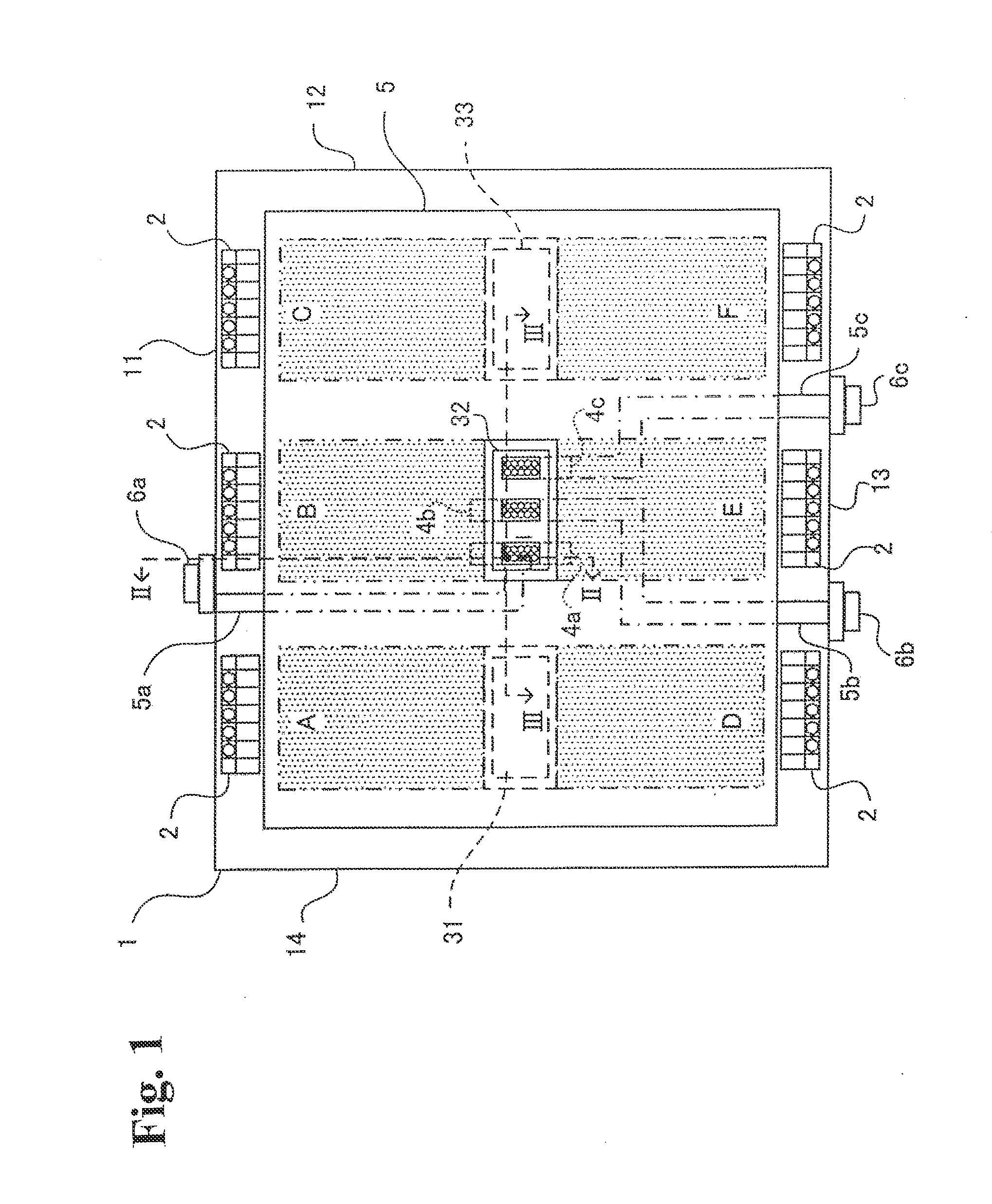
[0022]Hereafter, referring to the drawings, a description will be made to an embodiment of the invention. FIG. 1 is a top plan view showing a semiconductor device according to the embodiment of the invention.

[0023]The semiconductor device has circuit, formation regions A to F, shown by the two-dot. chain lines,, disposed by dividing the inside of a rectangular case 1 into, for example, six regions, and an inverter circuit configured by a semiconductor element, such as an IGBT, is disposed in each of the circuit formation regions A to F. A pair of inverter circuits is formed for each pair of circuit formation regions A and D, B and E, and C and F in the case 1.

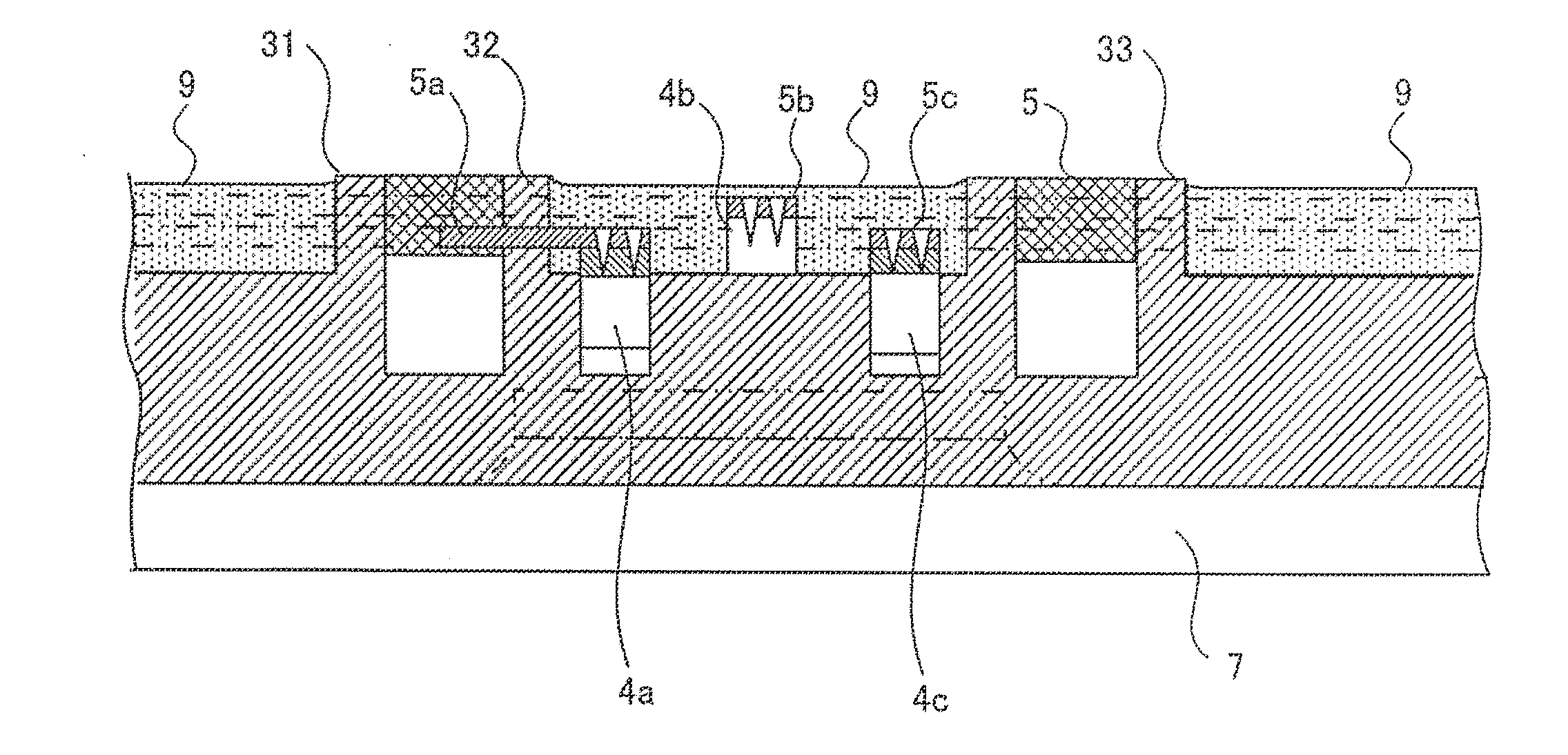
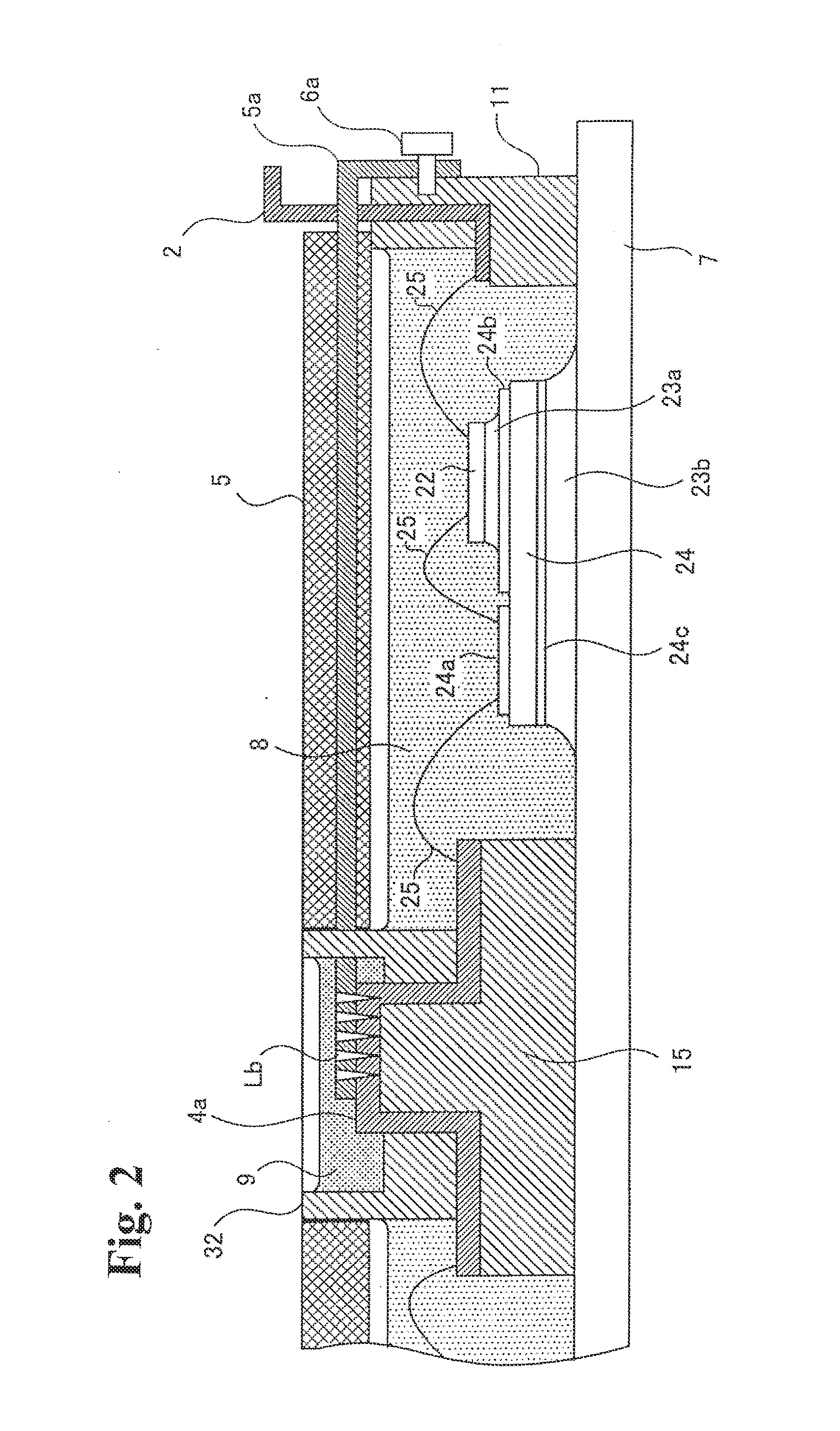
[0024]Control terminals 2 are terminals through, which control signals are supplied to the inverter circuits in the circuit formation regions A to F, and are embedded in corresponding front-back direction outer peripheral sidewalls 11 and 13 of the case 1 adjacent to their respective circuit formation regions A to C and D to F....


PUM


Abstract

Terminal assembly portions, lying on a front surface side of a case, are aligned in a left-right direction in a portion raised from a bottom of the case so that opening faces of the terminal assembly portions are positioned above circuit formation regions. Wiring terminal plates are led out into the terminal assembly portions, and disposed adjacent to each other. After each wiring terminal plate is connected by a laser welding to one end of one external connection terminal plate formed integrally with a cover, these welded portions are sealed with a second mold resin portion made of gel or an insulating resin such as epoxy. By so doing, even when the terminal junction area and distance between terminal junctions in the terminal assembly portions are small, it is possible to increase the joint strength of the terminals, and also secure withstand voltage.

Description

BACKGROUND OF THE INVENTION[0001]1. Technical Field[0002]The present invention relates to a semiconductor device having, in a case, a circuit formation region including a plurality of semiconductor elements, and to a method of manufacturing the semiconductor device, and particularly, relates to a semiconductor device wherein a plurality of semiconductor elements is electrically connected from wiring terminal plates embedded in the case through external connection terminal plates to external terminals formed on an outer peripheral portion of the case, and to a method of manufacturing the semiconductor device.[0003]2. Related Art[0004]In recent years, a reduction in size and weight of an inverter circuit which converts high electric power using a plurality of semiconductor elements such as insulated gate bipolar transistors (IGBTs) has been attempted. There is a description of a semiconductor device, such as a power module using a common IGBT module, in JP-A-08-148645 (for example, re...

Claims


Application Information

Patent Timeline
Patent Type & Authority Applications(United States)
IPC IPC(8): H01L23/00
CPCH01L2224/85H01L2924/3025H01L2224/45124H01L2224/32225H01L2224/48091H01L2224/48227H01L2224/73265H01L25/00H01L23/24H01L23/49811H01L23/3735H01L23/36H01L24/46H01L24/85H01L2924/13055H01L2924/12041H01L24/29H01L24/32H01L24/45H01L24/48H01L24/49H01L24/92H01L2224/291H01L2224/4911H01L2224/83801H01L2224/92247H01L2924/1305H01L2924/19107H01L2924/00012H01L2924/00014H01L2924/00011H01L2924/00H01L2924/181H01L2924/12042H01L24/73H01L2924/014
Inventor SUZUKI, KENJI
Owner FUJI ELECTRIC CO LTD
Why Eureka
Try Eureka