Pixel arrangement structure for organic light emitting display device

a technology of organic light emitting diodes and arrangement structures, which is applied in semiconductor devices, instruments, electrical devices, etc., can solve the problems of deteriorating deposition reliability and deteriorating aperture ratio of pixels, and achieve the effect of improving the aperture ratio of pixels and efficiently setting up the gap between pixels

Active Publication Date: 2013-09-12
SAMSUNG DISPLAY CO LTD
View PDF17 Cites 121 Cited by
  • Summary
  • Abstract
  • Description
  • Claims
  • Application Information

AI Technical Summary

Benefits of technology

[0027]According to an exemplary embodiment of the present invention, the pixel arrangement structure of the OLED display improves the aperture ratio of the pixel while efficiently setting up the gap between the pixels.

Problems solved by technology

When reducing a gap between the neighboring pixels to obtain a high aperture ratio of the pixel, deposition reliability may be deteriorated.
On the other hand, when increasing the gap between the pixels to improve the deposition reliability, the aperture ratio of the pixel may be deteriorated.

Method used


Image

  • Pixel arrangement structure for organic light emitting display device
  • Pixel arrangement structure for organic light emitting display device
  • Pixel arrangement structure for organic light emitting display device

Examples


Embodiment Construction

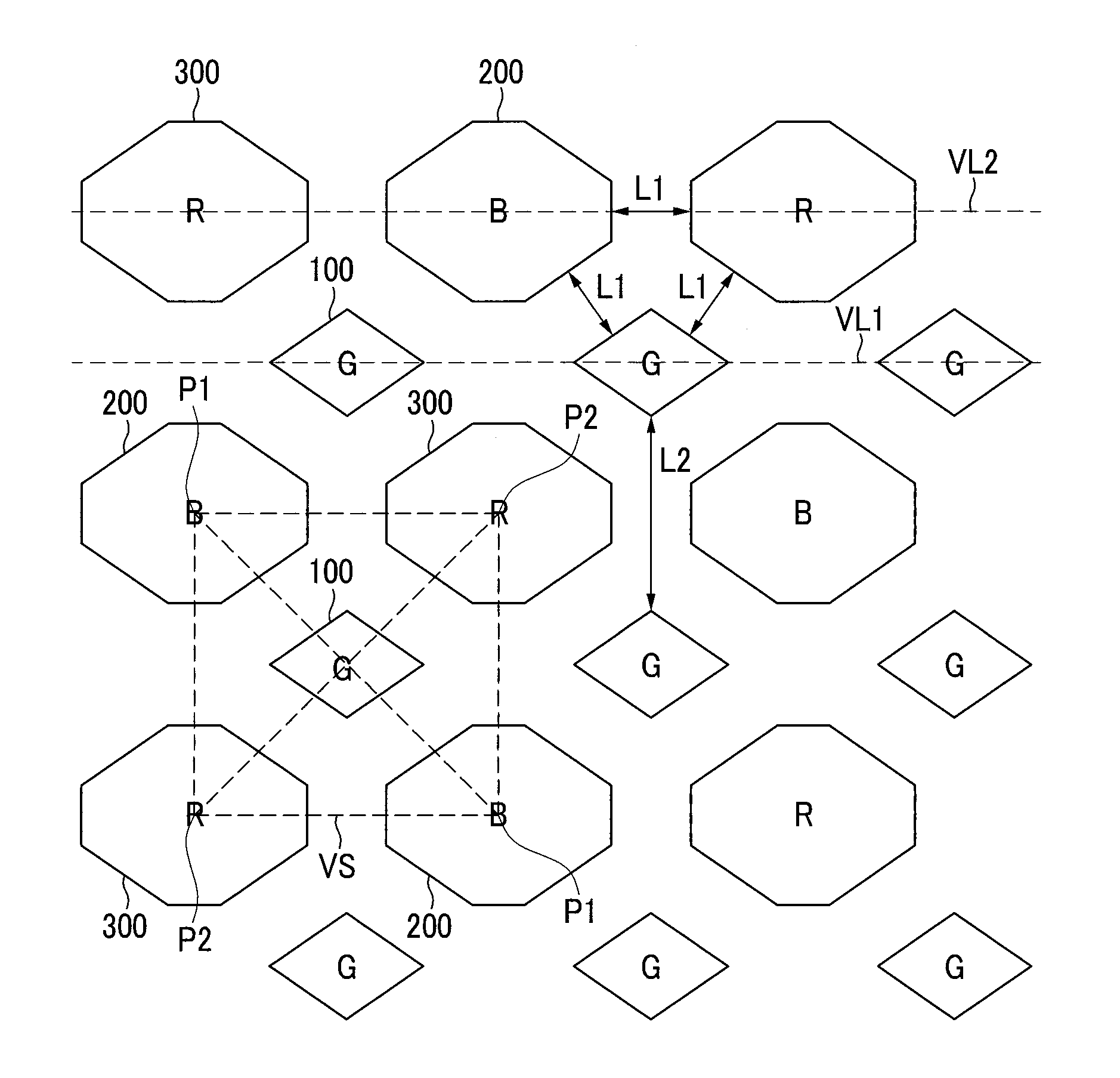
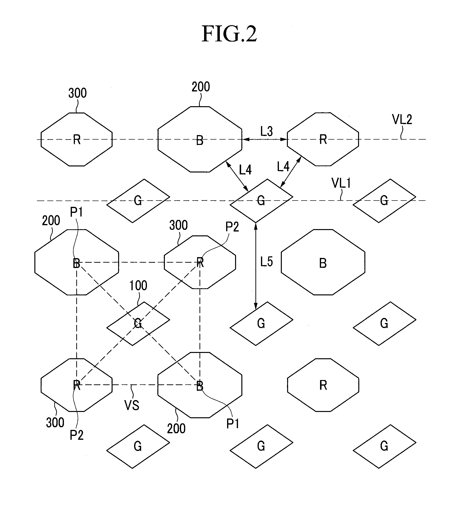
[0033]Several exemplary embodiments according to the present invention are described hereinafter in detail with reference to the accompanying drawings to allow one of a person of ordinary skill in the art to practice the invention without undue experimentation. The present invention can be embodied in several different forms, and is not limited to exemplary embodiments that are described herein.

[0034]In order to clarify the description of embodiments of the present invention, parts that are not related to the embodiments may be omitted. In addition, the same elements or equivalents are referred to with the same reference numerals throughout the specification. For example, the same reference numerals are used for the elements having the same constructions throughout. Such elements are representatively described in a first exemplary embodiment, and in remaining exemplary embodiments, only different constructions from those of the first exemplary embodiment may be described.

[0035]Furth...


PUM


Abstract

A pixel arrangement structure of an OLED display is provided. The pixel arrangement structure includes: a first pixel having a center coinciding with a center of a virtual square; a second pixel separated from the first pixel and having a center at a first vertex of the virtual square; and a third pixel separated from the first pixel and the second pixel, and having a center at a second vertex neighboring the first vertex of the virtual square.

Description

CROSS-REFERENCE TO RELATED PATENT APPLICATION[0001]This application claims priority to and the benefit of Korean Patent Application No. 10-2012-0022967, filed in the Korean Intellectual Property Office on Mar. 6, 2012, the entire content of which is incorporated herein by reference.BACKGROUND[0002]1. Field[0003]Aspects of embodiments of the present invention relate generally to a pixel arrangement structure of an organic light emitting diode (OLED) display.[0004]2. Description of the Related Art[0005]A display device is a device that displays an image. Recently, an OLED display has been drawing attention. The OLED display has a self-luminous characteristic. Because the OLED display does not need a separate light source, unlike a liquid crystal display, it can have a relatively smaller thickness and weight than liquid crystal displays. In addition, the OLED display exhibits high-quality characteristics such as low power consumption, high luminance, high response speed, etc.[0006]In g...

Claims


Application Information

Patent Timeline
Patent Type & Authority Applications(United States)
IPC IPC(8): G09G3/32
CPCH01L27/3218H01L27/3216H10K59/352H10K59/353H10K50/805
Inventor LEE, SANG-SHIN
Owner SAMSUNG DISPLAY CO LTD
Why Eureka
Try Eureka