
Antenna and combination antenna
- Summary
- Abstract
- Description
- Claims
- Application Information
AI Technical Summary
Benefits of technology
Problems solved by technology
Method used
Image

Examples
first embodiment
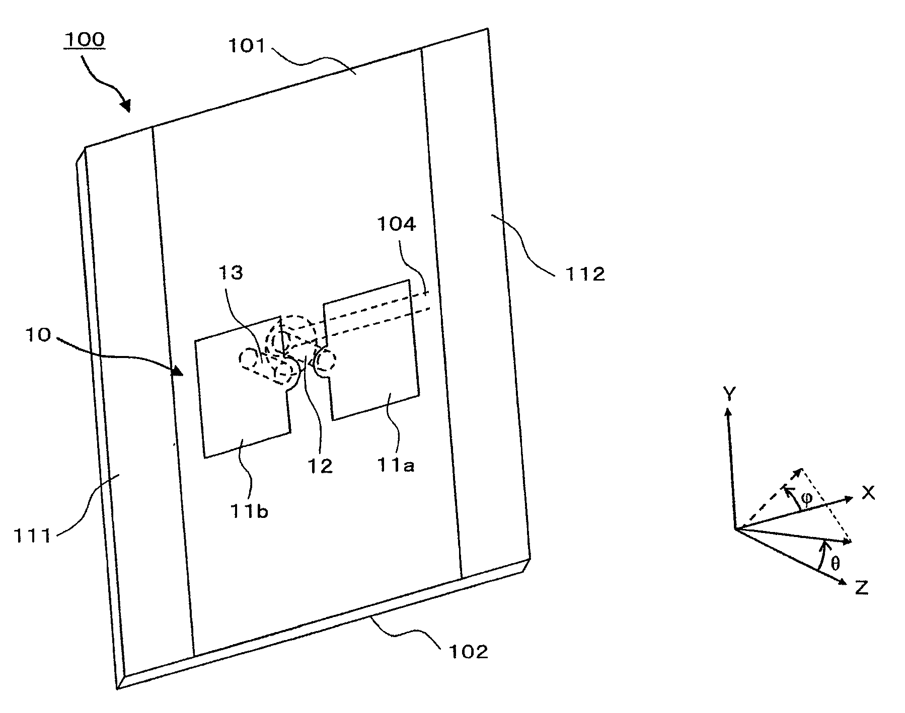
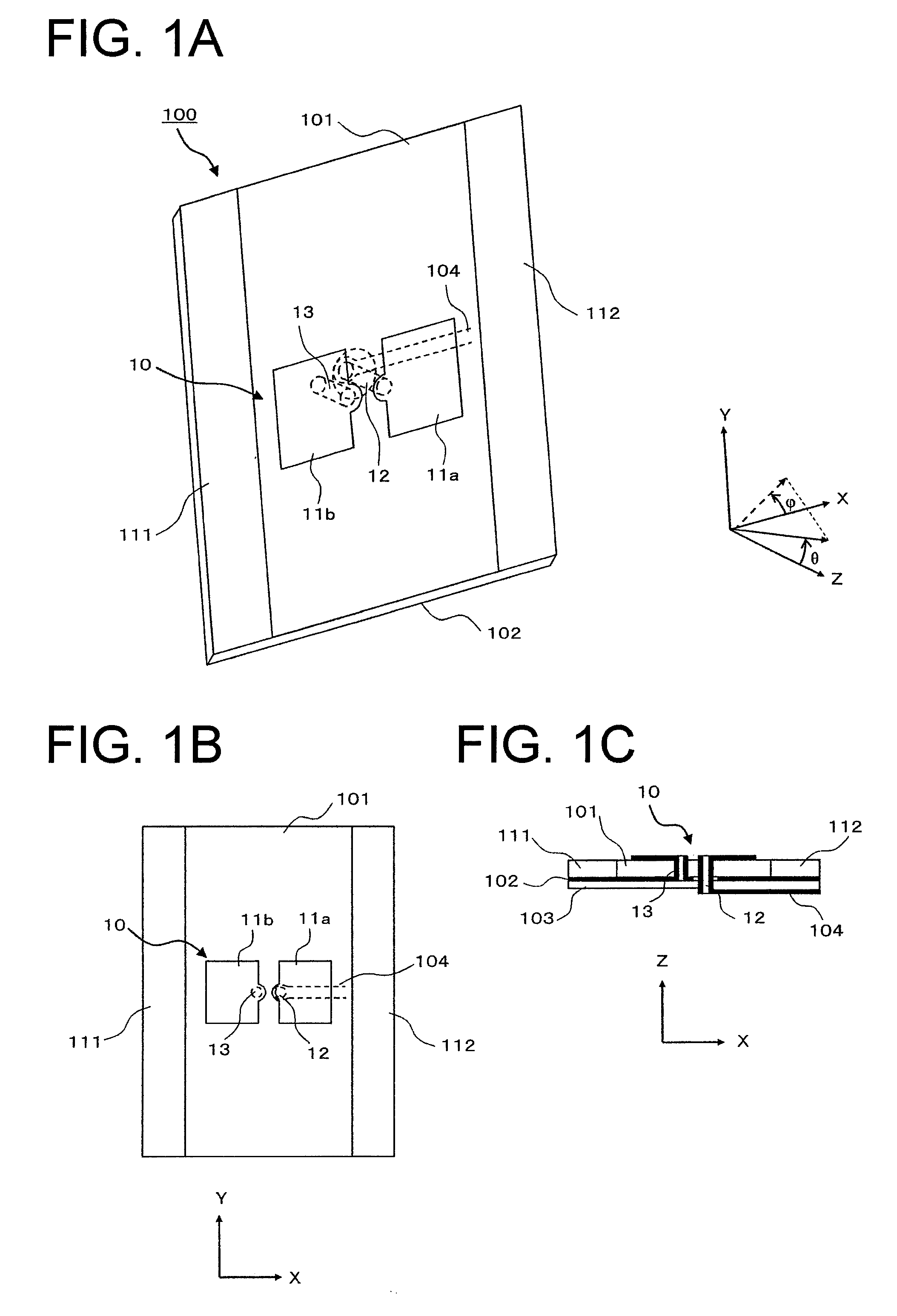
[0073]Then, in the antenna and combination antenna of the present invention, for the purpose of suppressing of TM surface wave on the dielectric substrate 101 and shaping of the radiation pattern, a rim made of a metal plate or EBG (Electromagnetic Band Gap) is arranged near the antenna element 10 arranged in the X direction (horizontal direction). EBG has two types of coplanarity type and mushroom type, either of which is selected to be used according to the situation. In the combination antenna of the present invention, whichever EBG is used, the same function is obtained. Therefore, these are not distinguished in the following description. First, the antenna according to the present invention is described with reference to FIG. 1. FIGS. 1A to 1C are views each illustrating the structure of the antenna 100 of the present embodiment. FIGS. 1A to 1C are a perspective view, a plan view and a cross sectional view of the antenna 100.
[0074]The antenna 100 of the present embodiment shown...
second embodiment
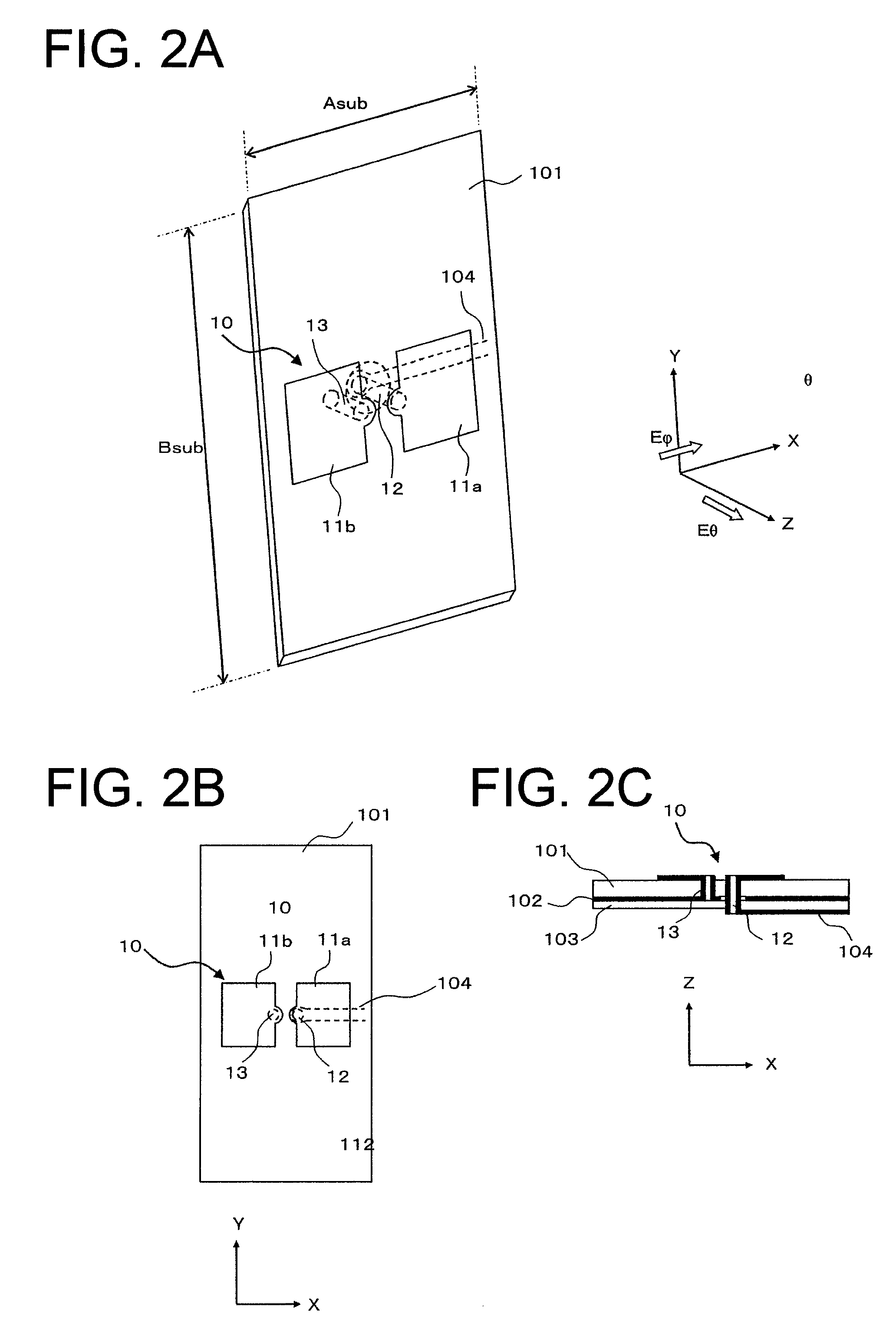
[0076]Next description is made, with reference to FIGS. 8A and 8B, about an antenna according to the present invention. FIGS. 8A and 8B are plan views illustrating the structures of antennas 200a and 200b of this embodiment. The antenna 200a of this embodiment shown in FIG. 8A is an array antenna composed of a phase-comparison monopulse antenna 20 having two antenna elements arranged in a 1×2 pattern, and the array antenna is sandwiched by rims 201a and 202a at both ends in the X direction of the dielectric substrate 101. In addition, FIG. 8B illustrates the antenna 200b which is the monopulse antenna 20 of the same size provided with rims 201b and 202b of different size.
[0077]In the antenna 200a shown in FIG. 8A, the width Asub of the dielectric substrate 101 (length in the X direction) is 11 mm, the widths of the rims 201a, 202a arranged left and right are both 4.5 mm, and the total width A becomes 20 mm. In addition, in the antenna 200b shown in FIG. 8B, the width Asub of the die...
third embodiment
[0081]An antenna according to the present invention will be described with reference to FIG. 10. FIG. 10 is a plan view illustrating the structure of the antenna 210 of the present embodiment. The antenna 210 of the present embodiment is structured as a linear array antenna in which four antenna elements 10 are arranged on a dielectric substrate 211 in a line (4×1 pattern). At its left and right sides (X direction), rims 212 and 213 are provided. The width Asub of the dielectric substrate 211 is 8.5 mm and the total width A including the rims 212, 213 is 34 mm. The reference numeral 214 denotes a transmission line which is formed on the back surface of the antenna 210 to be connected to each of the antenna elements 10. The antenna 210 is used as a transmission antenna for a radar device.
[0082]As to the radiation pattern of the linear array antenna 210 of the present embodiment, its simulation analysis results are shown in FIGS. 11A and 11B by S31. FIG. 11A shows Az patterns of the E...
PUM
 Abstract
Description
Claims
Application Information