Signal processing device, liquid crystal apparatus, electronic equipment, and signal processing method
a liquid crystal apparatus and signal processing technology, applied in the direction of electric digital data processing, instruments, computing, etc., can solve the problems of display defects, display contradictions likely to be perceived by users, display defects, etc., and achieve the effect of suppressing the occurrence of display defects
- Summary
- Abstract
- Description
- Claims
- Application Information
AI Technical Summary
Benefits of technology
Problems solved by technology
Method used
Image

Examples
first embodiment
[0067]First, a description will be made of the first embodiment of the invention.
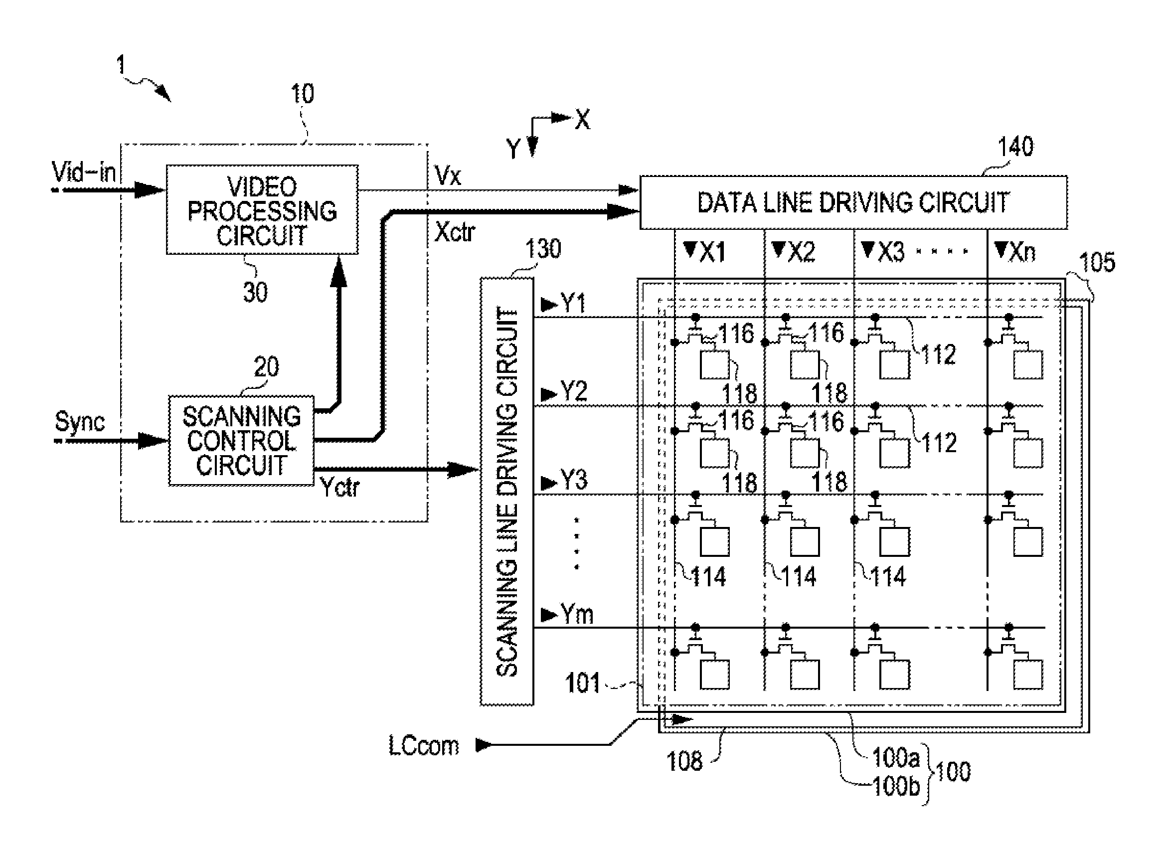
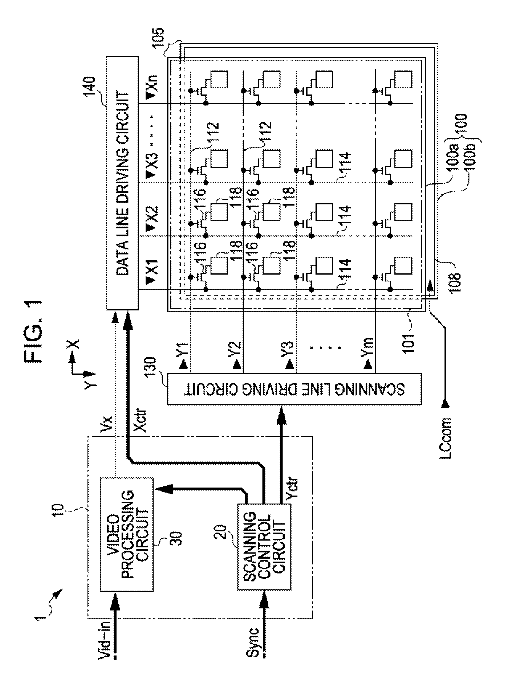
[0068]FIG. 1 is a block diagram illustrating an entire configuration of a liquid crystal display apparatus 1 which employs a video processing circuit according to the present embodiment.
[0069]As shown in FIG. 1, the liquid crystal display apparatus 1 includes a control circuit 10, a liquid crystal panel 100, a scanning line driving circuit 130, and a data line driving circuit 140. A video signal Vid-in is supplied to the control circuit 10 from a high rank device in synchronization with synchronization signals Sync. The video signal Vid-in is digital data which designates a grayscale level of each pixel of the liquid crystal panel 100, and is supplied in order of scanning according to a vertical scanning signal, a horizontal scanning signal, and a dot clock signal (neither shown) included in the synchronization signals Sync.
[0070]In addition, the video signal Vid-in designates, but an applied voltage to...
modification examples of first embodiment
Modification Example 1 of First Embodiment
[0131]In the above-described first embodiment, the correction portion 306 sets only a pixel adjacent to an applied boundary as a correction target dark pixel. Alternatively, the correction portion 306 may set two or more dark pixels (here, three) which are continuously located in an opposite direction to an applied boundary from a dark pixel adjacent to the applied boundary as a correction target as shown in FIG. 9. In this case, a time interval when a display screen of the liquid crystal panel 100 is updated is indicated by S (milliseconds), and a response time until the liquid crystal element 120 is turned to an alignment state when an applied voltage varies from a voltage lower than the judgment voltage Vjb to a voltage Vcb is indicated by U1 (milliseconds), the number of pixels is preferably equal to or more than a value which is obtained by adding 1 to a value of an integer part of a value obtained by dividing the response time U1 by th...
modification example 2 of first embodiment
[0138]In the above-described first embodiment, in a case where a potential difference between adjacent dark pixel and bright pixel is relatively small, and a correction voltage corresponding to the dark pixel is made to be decreased, there are cases where a reverse tilt domain occurs even if a transverse electric field between the dark pixel and the bright pixel is weak after the next frame. For example, an image line is considered in which a plurality of continuous dark pixels and a plurality of continuous bright pixels are arranged in a line, for example, as shown in the N-th frame of FIG. 10A. Here, in a case where a dark pixel p1 with a grayscale level “bk” and a bright pixel p2 with a grayscale level “th2” are adjacent to each other, the dark pixel p1 is originally corrected to a video signal with a grayscale level cbmin. However, as shown in FIG. 10A, a bright pixel p3 with a grayscale level “wt” is adjacent to the bright pixel p2 on an opposite side to the dark pixel p1, and,...
PUM
| Property | Measurement | Unit |
|---|---|---|
| frequency | aaaaa | aaaaa |
| transmittance | aaaaa | aaaaa |
| transmittance | aaaaa | aaaaa |
Abstract
Description
Claims
Application Information
 - R&D Engineer
- R&D Manager
- IP Professional
- Industry Leading Data Capabilities
- Powerful AI technology
- Patent DNA Extraction
Browse by: Latest US Patents, China's latest patents, Technical Efficacy Thesaurus, Application Domain, Technology Topic.
© 2024 PatSnap. All rights reserved.Legal|Privacy policy|Modern Slavery Act Transparency Statement|Sitemap