
Pixel array and display panel

Active Publication Date: 2013-10-03
AU OPTRONICS CORP
View PDF6 Cites 2 Cited by
  • Summary
  • Abstract
  • Description
  • Claims
  • Application Information

AI Technical Summary

Benefits of technology

The patent is about a new pixel array and display panel that can improve display quality. The two thin-film transistors in the array have the same projection patterns, which means that they will have the same variations in capacitance when a shift occurs during manufacturing. As a result, the feed-through voltages of neighboring sub-pixels will remain the same, and the display panel will have a better display quality.

Problems solved by technology

However, as the development of display panel follows the trend of becoming larger in size, when an exposing process is performed using a photomask for manufacturing a large display panel, since overall accuracy of large photomask is difficult to control due to factors like thermal expansion and cold shrinkage, overlapping alignment error (or overlay variation) in each metal layer of the thin-film transistor may easily become larger.
As a result, the display quality of the display panel may be affected thereby.

Method used


Image

  • Pixel array and display panel
  • Pixel array and display panel
  • Pixel array and display panel

Examples


first embodiment

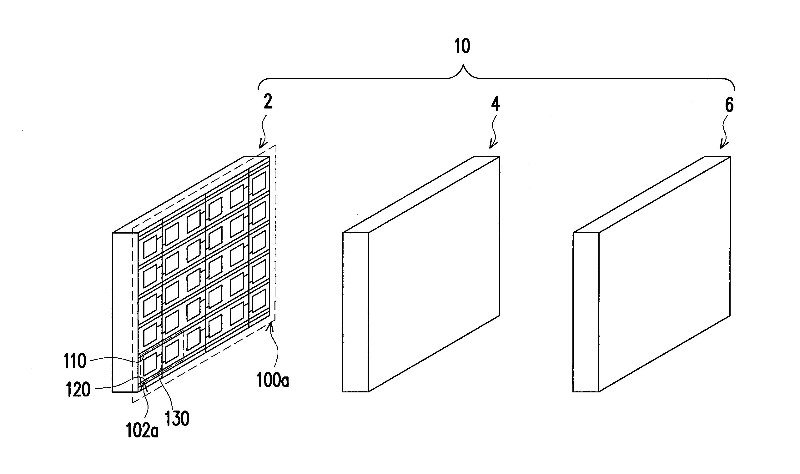
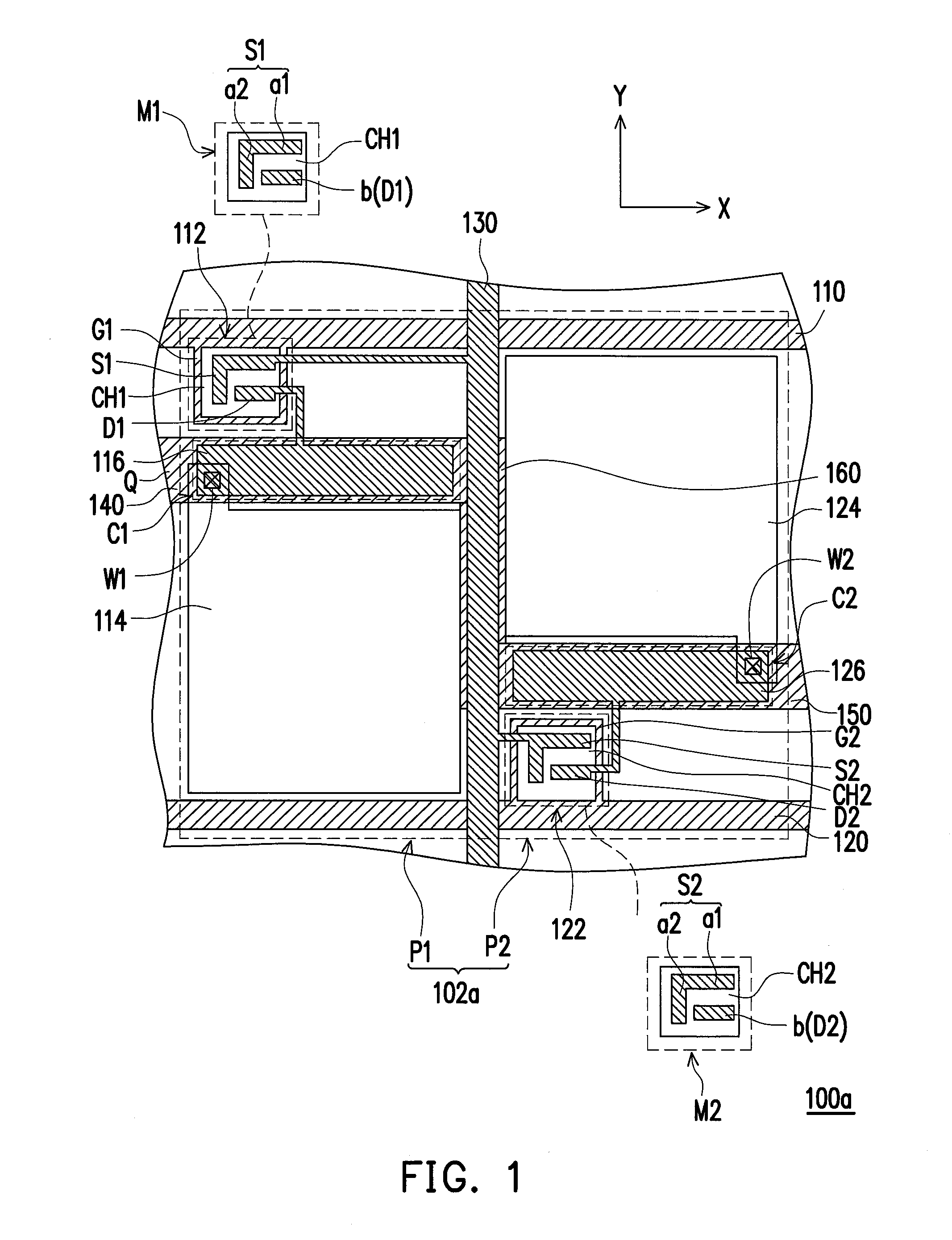
[0019]FIG. 1 is a partial view of a pixel array according to the first embodiment of the invention. Referring to FIG. 1, the pixel array 100a of the present embodiment includes a plurality of pixel units 102a. Herein, although FIG. 1 illustrates only one pixel unit 102a, however, those skilled in the art may understand the structure of the pixel array 100a of the invention, by the structure shown in FIG. 1 and the following description.

[0020]The pixel unit 102a includes a first sub-pixel P1 and a second sub-pixel P2, wherein the first sub-pixel P1 includes a first scan line 110, a data line 130, a first thin-film transistor 112, and a first pixel electrode 114. The second sub-pixel P2 includes a second scan line 120, the data line 130, a second thin-film transistor 122 and a second pixel electrode 124. According to the present embodiment, the first sub-pixel P1 and the second sub-pixel P2 share the data line 130, thereby forming a HSD pixel structure.

[0021]The material of the first ...

second embodiment

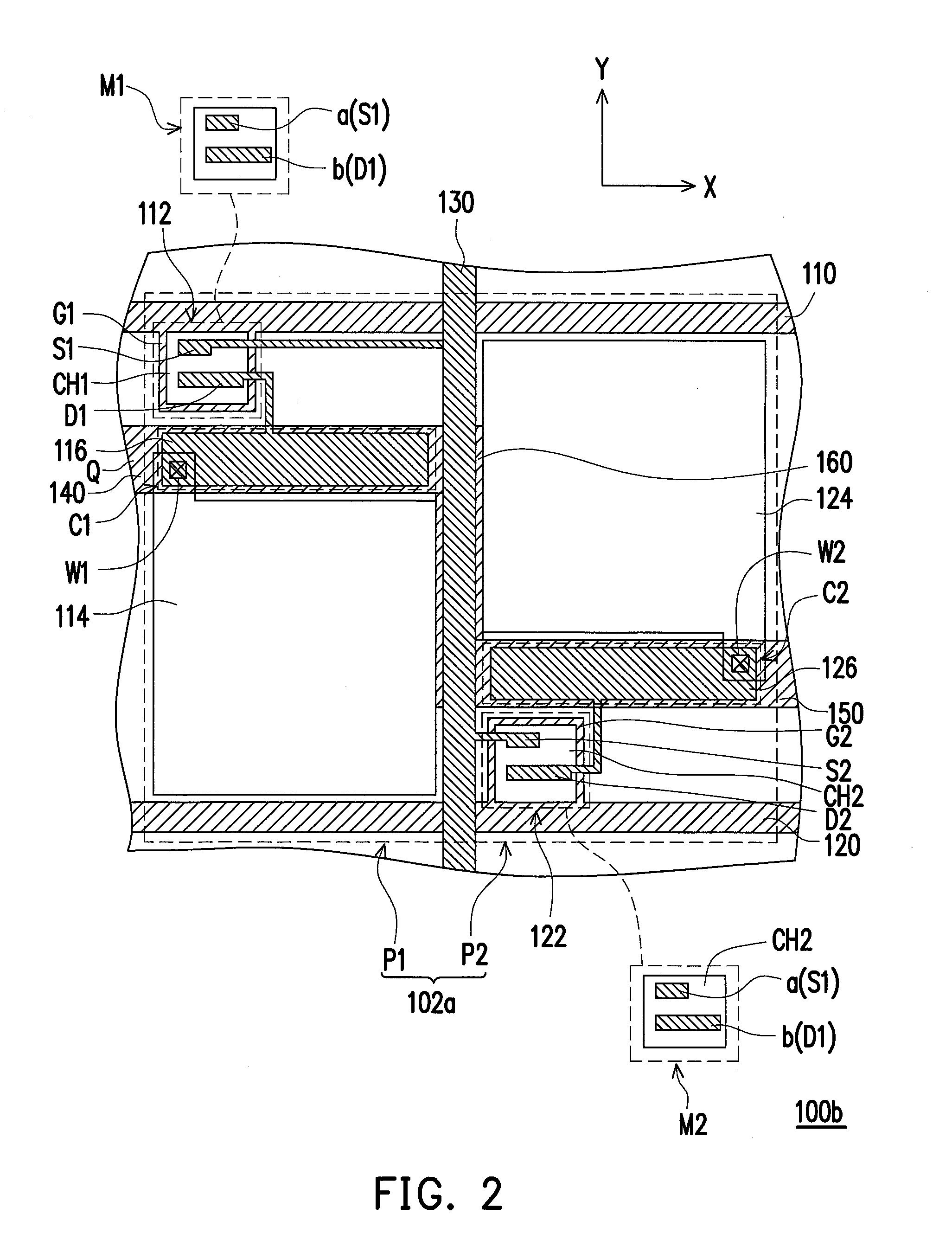
[0038]FIG. 2 is a partial view of a pixel array according to the second embodiment of the invention. Referring to FIG. 2, the pixel array 100b of the present embodiment is similar to the pixel array 100a of the first embodiment, their difference lies where the layout design of the thin-film transistor of the pixel array 100b is different from the layout design of the thin-film transistor of the pixel array 100a. It is noted that, components with same reference numerals represent same or similar components in the following embodiment, and the description to the same are omitted accordingly. The layout designs of the first thin-film transistor 112 and the second thin-film transistor 122 of the pixel array 100b are described in detail as below.

[0039]Referring to the enlarged diagram of part Ml in FIG. 2, the first source electrode S1 of the first thin-film transistor 112 of the present embodiment, for example, is composed by one conductor portion a, wherein the conductor portion a, for...

third embodiment

[0042]FIG. 3 is a partial view of a pixel array according to the third embodiment of the invention. Referring to FIG. 3, the pixel array 100c of the present embodiment is similar to the pixel array 100a of the first embodiment, their difference lies where the layout design of the thin-film transistor of the pixel array 100c is different from the layout design of the thin-film transistor of the pixel array 100a. The layout designs of the first thin-film transistor 112 and the second thin-film transistor 122 of the pixel array 100c are described in detail as below.

[0043]Referring to the enlarged diagram of part M1 in FIG. 3, the first source electrode S1 of the first thin-film transistor 112 of the present embodiment, for example, is composed by one conductor portion a, wherein the conductor portion a is a U-shaped conductor having an opening towards X direction. Moreover, the first drain electrode D1, for example, is composed by one conductor portion b, wherein the conductor portion ...


PUM


Abstract

A pixel array and a display panel are provided. The pixel array includes a plurality of pixel units. Each of the pixel units includes a first scan line, a second scan line, a data line, a first thin-film transistor, a second thin-film transistor, a first pixel electrode and a second pixel electrode. The first thin-film transistor is electrically connected to the first scan line and the data line. The first pixel electrode is electrically connected to the first thin-film transistor. The second thin-film transistor is electrically connected to the second scan line and the data line. The second pixel electrode is electrically connected to the second thin-film transistor. The orthogonal projection pattern of the first thin-film transistor on XY plane and the orthogonal projection pattern of the second thin-film transistor on XY plane are substantially the same.

Description

CROSS-REFERENCE TO RELATED APPLICATION[0001]This application claims the priority benefit of Taiwan application serial no. 101111419, filed on Mar. 30, 2012. The entirety of the above-mentioned patent application is hereby incorporated by reference herein and made a part of this specification.BACKGROUND OF THE INVENTION[0002]1. Field of the Invention[0003]The invention relates to a pixel structure and more particularly to a pixel array having a half source driving (HSD) structure.[0004]2. Description of Related Art[0005]With the development of large display panel nowadays, the so called half source driving (HSD) structure is widely used for a pixel array structure of liquid crystal display. Since the number of data lines may be reduced to half by using the HSD pixel structure, the price of the source driver is reduced accordingly. More specifically, the HSD structure includes a plurality of pixel units, each of the pixel units includes two neighbouring sub-pixels which share one data...

Claims


Application Information

Patent Timeline
IPC IPC(8): H01L33/08
CPCG02F1/1362G02F1/136213G02F1/13624G02F1/136286H01L27/124H01L27/1255
Inventor CHEN, SZU-CHIEHTING, YU-HSINCHEN, CHEN-MINGCHEN, I-FANGHUNG, YI-XUANFAN, DA-WEI
Owner AU OPTRONICS CORP
Learn More