

Thin film transistor substrate and manufacturing method for the same
- Summary
- Abstract
- Description
- Claims
- Application Information
AI Technical Summary
Benefits of technology
Problems solved by technology
Method used
Image

Examples
first preferred embodiment
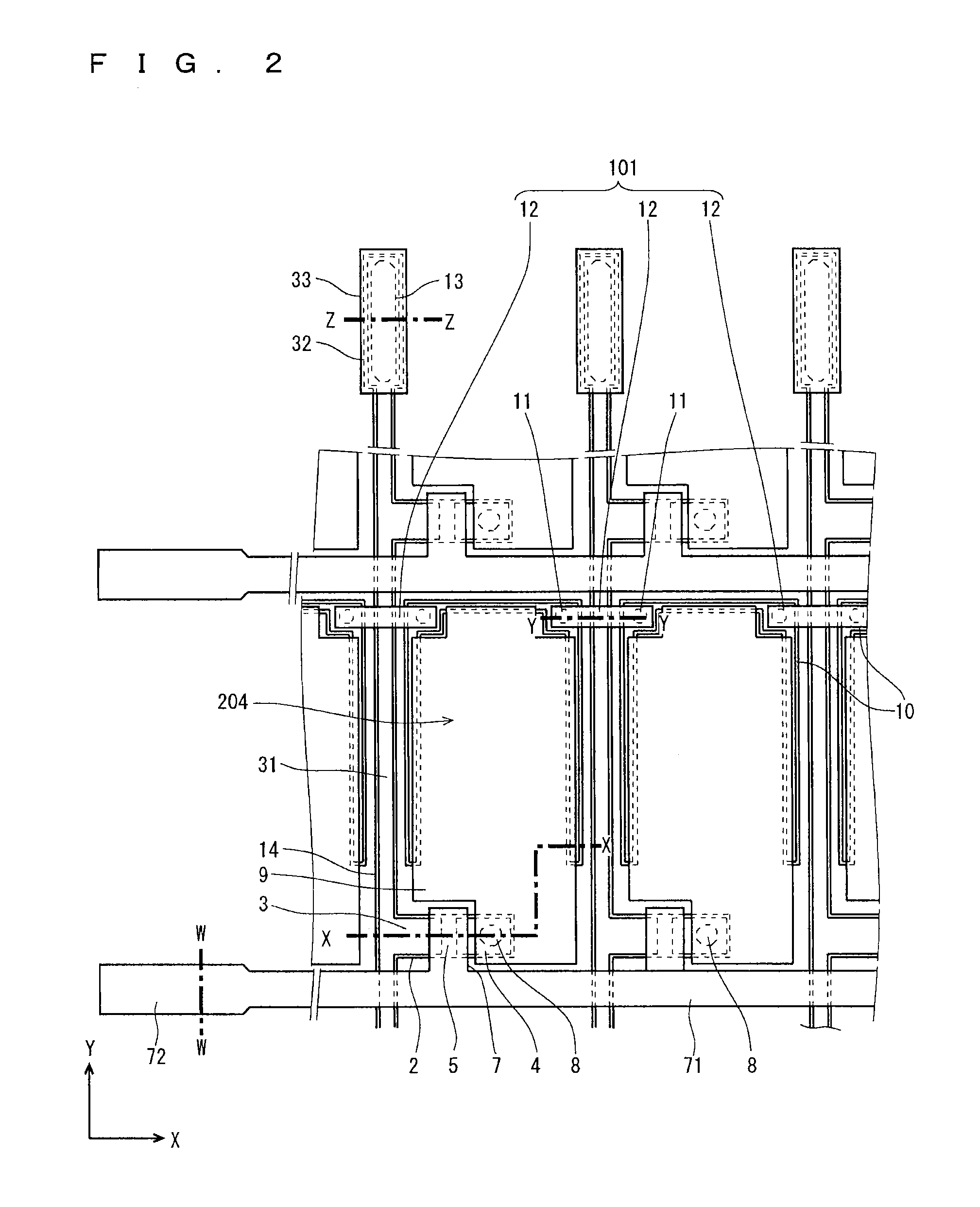
[0040]A TFT substrate according to the present preferred embodiment will be described as an active matrix substrate using a thin film transistor as a switching element.
[0041]It is to be noted that the TFT substrate is used for a flat-type display (flat panel display) such as a liquid crystal display (LCD).
[0042]
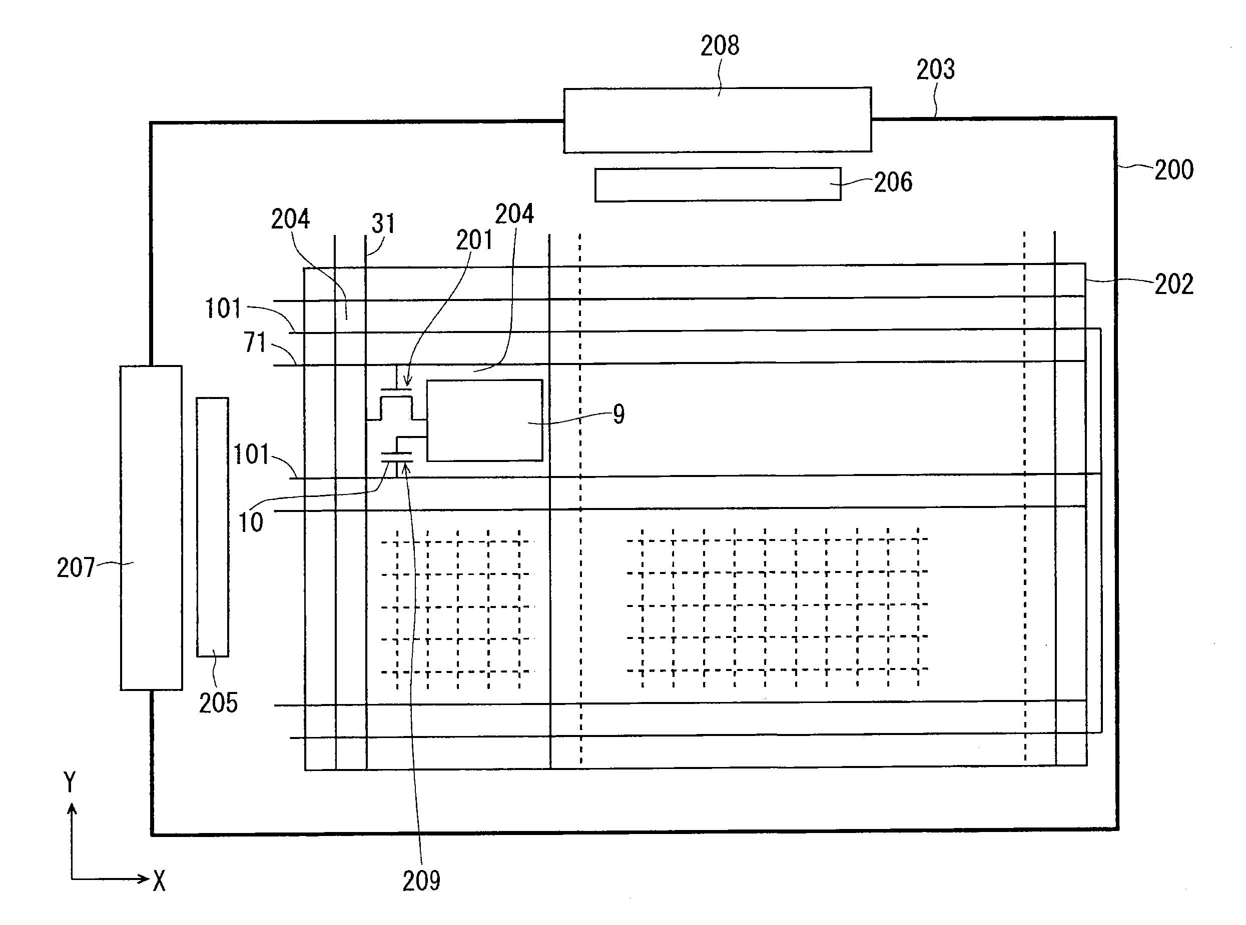
[0043]First, an overall configuration of the TFT substrate will be described using FIG. 1. FIG. 1 is a plan view schematically describing an overall configuration of a TFT substrate, and herein, a TFT substrate for LCD is taken as an example.
[0044]A TFT substrate 200 shown in FIG. 1 is a TFT array substrate with TFTs 201 arrayed in matrix shape, and broadly divided into a display area 202 and a frame area 203 provided so as to surround the display area 202.
[0045]In the display area 202, a plurality of gate lines (scanning signal lines) 71, a plurality of auxiliary capacitance electrodes 10 and a plurality of source lines (display signal lines) 31 are disposed. The plurality o...
second preferred embodiment
[0123]The example has been described in above described the first preferred embodiment where the first conductive film 15 includes the Al alloy film, but in the TFT substrate 200 according to a second preferred embodiment, the first conductive film 15 includes a Cu film or a Cu alloy film mainly containing Cu. Hereinafter, the Cu film and the Cu alloy film mainly containing Cu are collectively called a Cu film. In addition, other than the above, the same configuration as in the first preferred embodiment is provided with the same numeral, and a repeated description will be omitted.
[0124]
[0125]Next, a manufacturing method for the TFT substrate 200 according to the second preferred embodiment will be described using FIGS. 4, 5 and 16 to 22. It is to be noted that a sectional view showing a final step corresponds to FIG. 3, and each of the parts (a) to (d) in FIG. 3 indicates the same portion in each sectional view describing the manufacturing process in the following descriptions.
[012...
modified example
[0145]Although pure Cu has been used as the material for the first metal film 15, the material for the first metal film 15 is not restricted to this. For example a Cu alloy film obtained by adding any one of Ti, V, Cr, Mn, Fe and Ni to Cu may be used.
[0146]As an upper limit of an additive amount of the additive, not higher than 10 mol % is taken as a guide in consideration of line resistance. Further, a lower limit is set so as to be a minimum amount required for depositing the additives as a surface protective layer by thermal treatment at 200 to 350° C. performed after pattern formation of the Cu alloy film, and for example, when the surface protective film has a film thickness being on the order of 1% of a film thickness of the Cu alloy film (2 nm when the film thickness of the Cu alloy is 200 nm), an atomicity ratio is set to 1 at % (=1 mol %).
[0147]These Cu alloy films are subjected to thermal treatment at 200 to 350° C., thereby to deposit an added element on the surface of th...
PUM
 Abstract
Description
Claims
Application Information