Substrate for a display device, a method for repairing the same, a method for repairing a display device and a liquid-crystal display device

Active Publication Date: 2008-06-19
SHARP KK
View PDF12 Cites 5 Cited by
  • Summary
  • Abstract
  • Description
  • Claims
  • Application Information

AI Technical Summary

Benefits of technology

[0012]The present invention was made in view of the aforementioned circumstances and aims at providing substrate for a display device, a method for repairing the same, a method for repairing a display device including the substrate for a display device and a liquid-crystal display device which enable making a portion suffering from a vertical leakage

Problems solved by technology

Although the relocation of the connecting portion between electrode slits to outside the light-blocking region causes concern about an alignment d

Method used


Image

  • Substrate for a display device, a method for repairing the same, a method for repairing a display device and a liquid-crystal display device
  • Substrate for a display device, a method for repairing the same, a method for repairing a display device and a liquid-crystal display device
  • Substrate for a display device, a method for repairing the same, a method for repairing a display device and a liquid-crystal display device

Examples


first embodiment

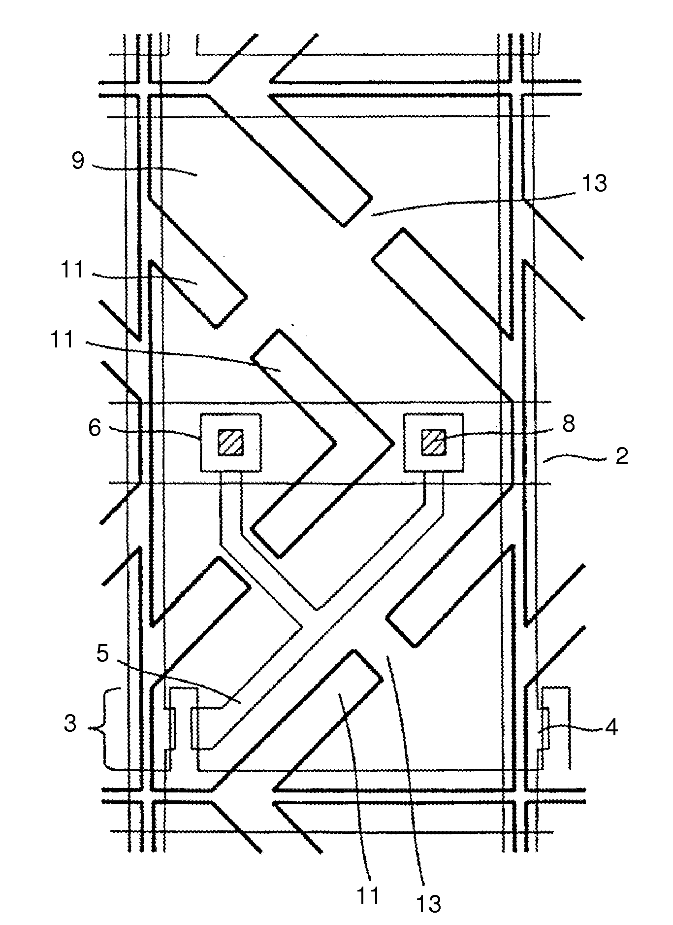
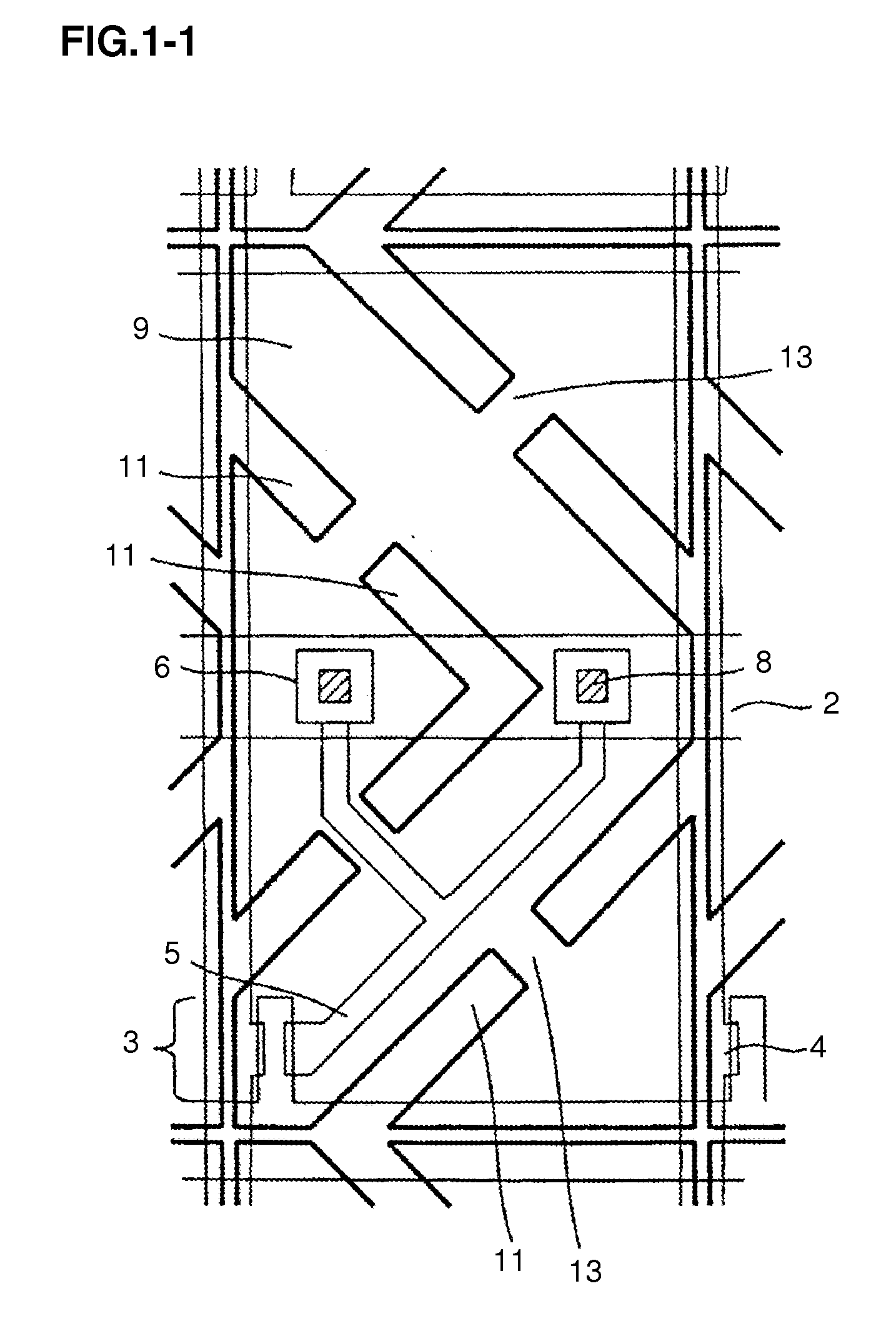
[0061]FIG. 2 is a cross sectional view schematically illustrating the configuration of a liquid crystal display device 100 according to the first embodiment of the present invention. FIG. 3 is a plan view schematically illustrating the shape of a pixel electrode on an active matrix substrate included in the liquid crystal display device 100 illustrated in FIG. 2.

[0062]The liquid crystal display device 100 includes a pair of opposing substrates, and a plastic bead or a column-shaped resin component provided on a color filter substrate 20, etc., are used as a spacer (not shown) to keep the space between the substrates constant. The liquid crystal display device 100 is an active-matrix type liquid crystal display device and includes the color filter substrate 20 and the active matrix substrate 30 including a switching device such as TFT.

[0063]Hereinafter, a method for fabricating the active matrix substrate 30 (AM substrate) 30 will be described.

[0064]A metal such as a Ti / Al / Ti laminat...

second embodiment

[0068]FIG. 4-1 is a plan view schematically illustrating the shape of pixel electrode on a CF substrate included in a liquid crystal display device according to the second embodiment of the present invention. In the present embodiment, it will be described that the present invention is applicable to a configuration in which a protrusion for vertical alignment 22 is provided on the electrode on the AM substrate of an MVA-type liquid crystal display device and the electrode 23 on the CF substrate opposing to the AM substrate is provided with a slit 11.

[0069]There is illustrated, in FIG. 4-1, the pattern of the opposed electrode 23 on the CF substrate according to the present embodiment which enables cutting off a portion suffering from a vertical leakage. In FIG. 4-1, a connecting portion between slits 25 is placed to surround an electrode region 24 and, in the event of occurrence of the vertical leakage within the electrode region 24, the portion suffering from the vertical leakage c...

third embodiment

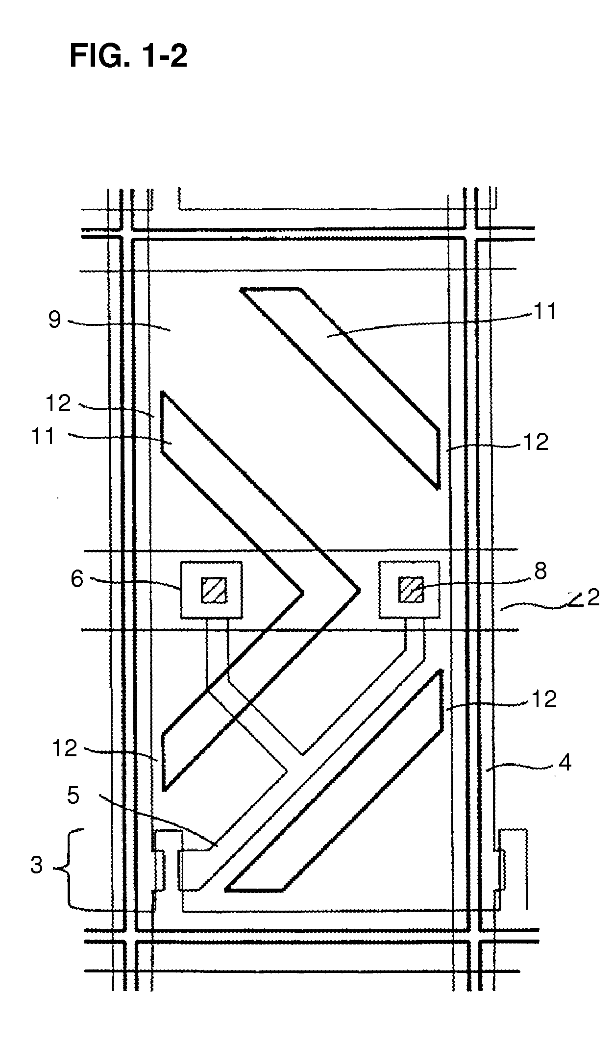
[0072]FIG. 5 is a plan view schematically illustrating the shape of pixel electrode on the substrate for a display device according to the third embodiment of the present invention.

[0073]In repairing a vertical leakage, the inter-electrode connecting portion is cut off by laser irradiation from the back surface of the substrate at the state where the TFT substrate and the CF substrate are attached to each other and therefore, when there exist a metal wiring between the connecting portion and the substrate, the metal wiring may be cut off together with the connecting portion. Therefore, the present invention is characterized in that the connecting portion is formed outside of the metal wiring. In the present embodiment, as illustrated in FIG. 5, in a pixel configuration including a plurality of independent contact holes 8, 8′ on the secondary wiring 2 for feeding a drain electric potential to the pixel electrode 9 wherein the respective contact holes 8, 8′ are connected to the drain ...


PUM


Abstract

The present invention is a substrate for a display device comprising an active matrix substrate and an opposed substrate which are opposed to each other with a display medium layer interposed therebetween, said active matrix substrate including a pixel electrode arranged in a matrix shape on the side of the display medium layer and said opposed substrate including a common electrode opposing to the pixel electrode on the side of the display medium layer, wherein said substrate for a display device includes an electrode slit formed in one of the pixel electrode and the common electrode; and at least one of the electrical connecting portions of said electrode slit is provided outside of a light-blocking region.

Description

BACKGROUND OF THE INVENTION[0001]1. Field of the Invention[0002]The present invention relates to a substrate for a display device, a method for repairing the same, a method for repairing a display device and a liquid crystal display device and, more particularly to a substrate for a display device which is suitably used in direct-vision type liquid crystal display devices such as a liquid crystal color television and projection-type liquid crystal display devices such as a liquid crystal projector, a method for repairing the same, a method for repairing a display device and a liquid crystal display device.[0003]2. Description of the Related Art[0004]As examples of liquid crystal display devices, there are color liquid crystal display devices including an active matrix (hereinafter, referred to as “AM”) substrate having a plurality of switching devices such as thin-film transistors (hereinafter, referred to as “TFTs”) formed thereon, a CF substrate having a color filter (hereinafter,...

Claims


Application Information

Patent Timeline
IPC IPC(8): G02F1/13G02F1/1343G02F1/133G02F1/1362G02F1/1368G09F9/30
CPCG02F1/133707G02F1/134309G02F1/136209G02F1/136213G02F2201/508G02F1/136259G02F1/1393G02F2001/134345G02F1/136227G02F1/134345G02F1/1343G02F1/1368
Inventor NAKAGAWA, HIDETOSHITSUBATA, TOSHIHIDENAGASHIMA, NOBUYOSHIHISADA, YUHKO
Owner SHARP KK
Why Eureka
Try Eureka