
On-chip transformer having multiple windings

a technology of on-chip transformers and windings, which is applied in the direction of transformers/inductance details, fixed transformers or mutual inductances, coils, etc., can solve the problems of large chip area, large chip area of passive devices such as inductors and transformers

Inactive Publication Date: 2013-10-10
REALTEK SEMICON CORP
View PDF8 Cites 34 Cited by
  • Summary
  • Abstract
  • Description
  • Claims
  • Application Information

AI Technical Summary

Benefits of technology

The present patent provides an on-chip transformer that includes a multi-winding structure and a guard ring surrounding it. The first and second windings function as a first transformer, and the second and third windings function as a second transformer. There are also windings that are separate from each other and wrap around each other. The vertical views upon the substrate of the second and third windings are located inside that of the outermost coil of the first winding. The technical effect is the integration of a transformer onto an integrated-circuit substrate, which reduces the size and complexity of the transformer while maintaining its functionality.

Problems solved by technology

If the transformer coils are realized in the form of integrated-circuit (IC) chip, they may spend a quite large chip area.
However, some passive devices like inductors and transformers often consume a large chip area.

Method used


Image

  • On-chip transformer having multiple windings
  • On-chip transformer having multiple windings
  • On-chip transformer having multiple windings

Examples


first embodiment

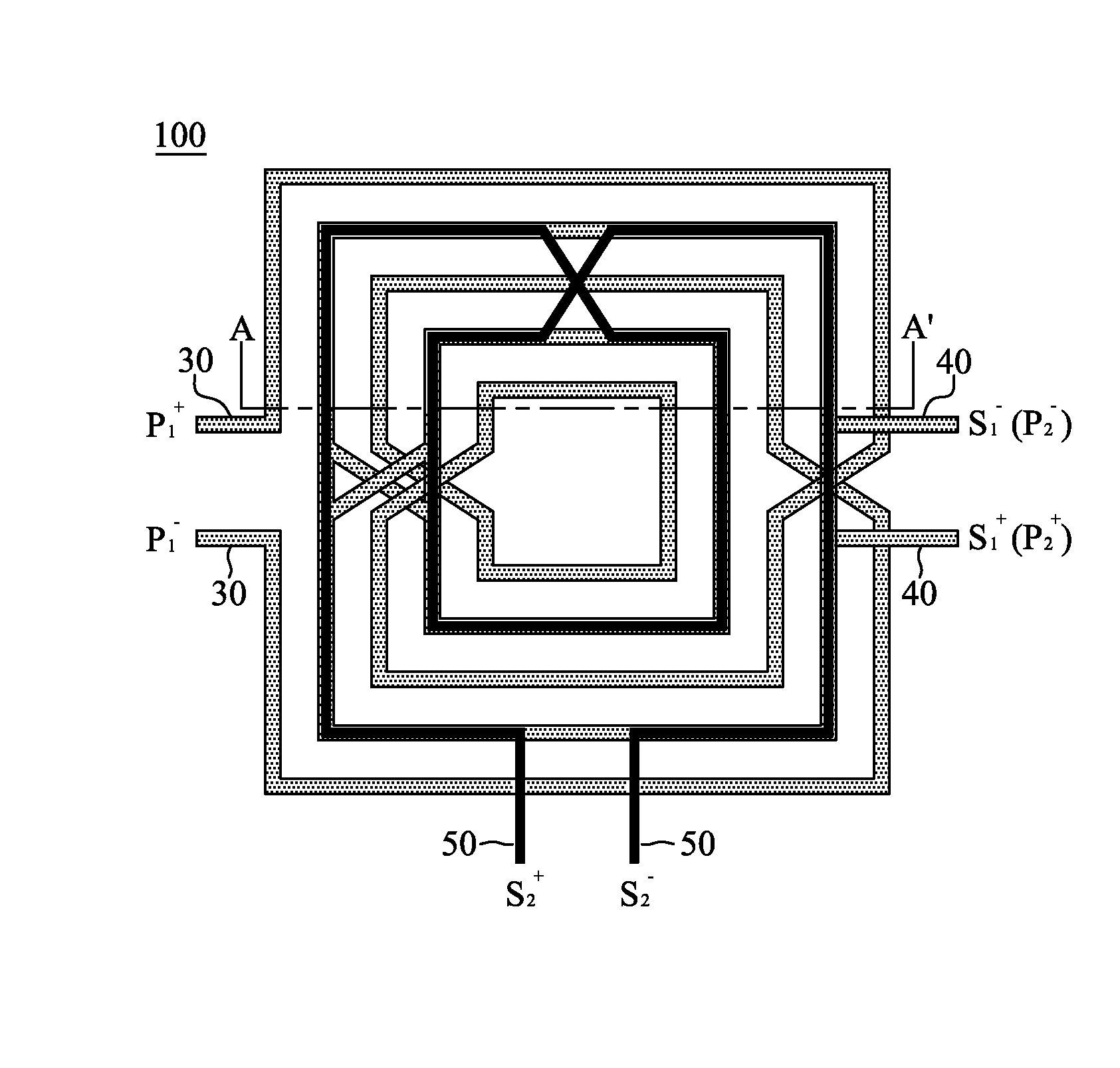
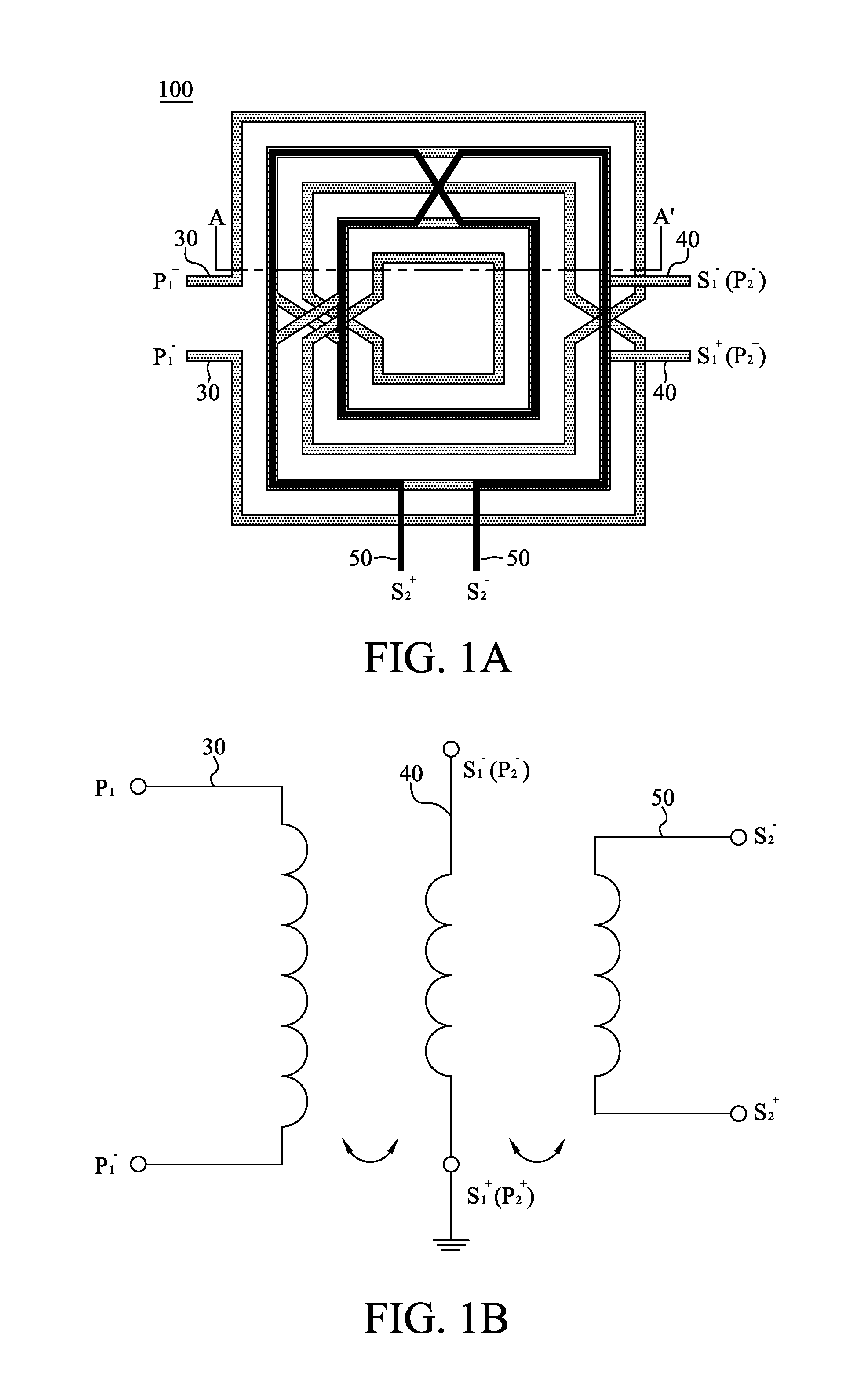
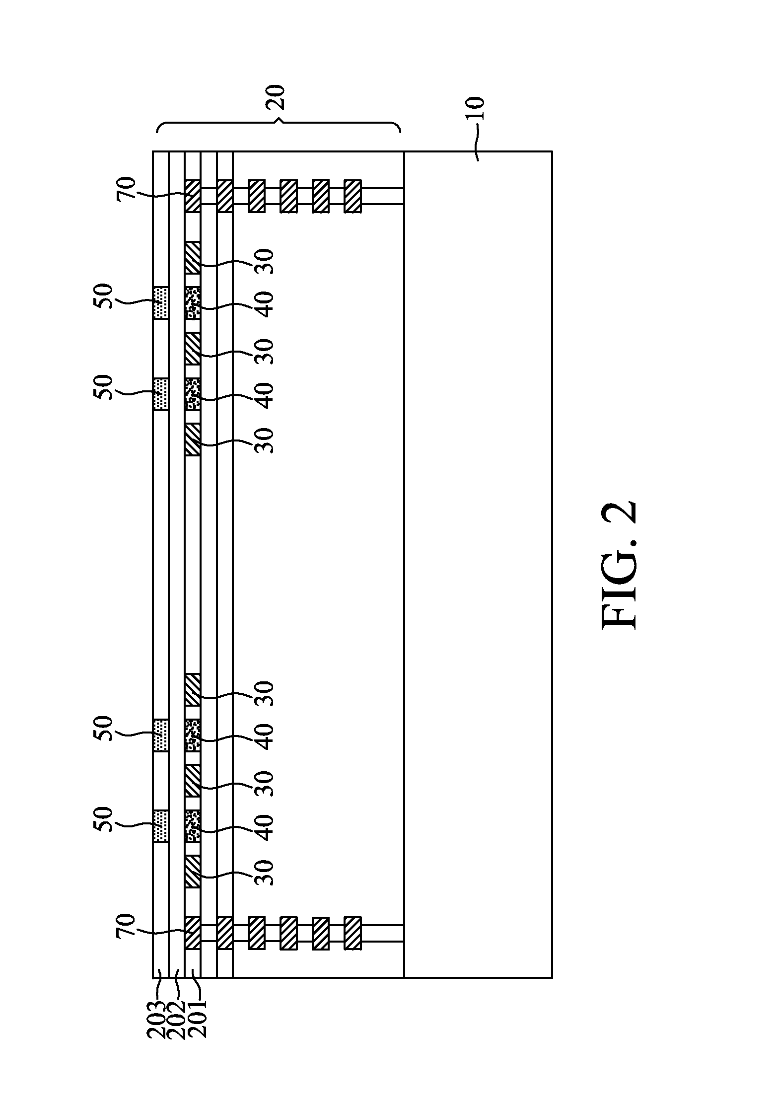
[0032]FIG. 1A schematically shows a vertical view of an on-chip transformer having multiple windings according to the present disclosure, and FIG. 2 is a cross-sectional diagram of the on-chip transformer taken along the A-A′ line in FIG. 1A. As shown in FIG. 1A, the on-chip transformer 100 comprises a multi-winding structure formed in a multi-layered structure 20 on a substrate 10. The multi-winding structure includes a first winding 30, a second winding 40, and a third winding 50, which are separated from each other. In another embodiment, the on-chip transformer 100 may further include a guard ring 70. Preferably, the guard ring 70 is composed of stacked metal rings surrounding the multi-winding structure and formed in the multi-layered structure 20, as shown in FIG. 2. The guard ring 70 can keep the on-chip transformer 100 isolated, so that the transformer inside the guard ring 70 and the devices outside the guard ring 70 may not interfere with each other electromagnetically. Fu...

fourth embodiment

[0044]Moreover, the foregoing three-winding transformer can be configured in another type of structure. FIG. 6 schematically shows a layout of an on-chip transformer having three windings according to the present disclosure. The on-chip transformer comprises a first winding 30, a second winding 40 and a third winding 50 formed in a multi-layered structure on a substrate. The windings 30 / 40 / 50 wrapping each other while separated from each other can be formed in a common layer or in several layers. If the windings 30 / 40 / 50 are formed in a common layer, they can form first and second transformers according to their respective lateral electromagnetic coupling effect therebetween.

[0045]In the above described embodiments, the electromagnetic coupling between two of the first, second and third winding 30, 40 and 50 can be lateral or vertical, according to their wiring patterns and layer distributions; this disclosure is not limited thereto.

[0046]The on-chip transformer according to the pre...


PUM

PropertyMeasurementUnit
direction angleaaaaaaaaaa
areaaaaaaaaaaa

Abstract

An on-chip transformer formed on an integrated-circuit substrate is disclosed. The on-chip transformer includes: a multi-winding structure comprising first, second and third windings which are spatially separated from each other; and a guard ring surrounding the multi-winding structure; wherein the first and second windings function as a first transformer, and the second and third windings function as a second transformer.

Description

CROSS-REFERENCE TO RELATED APPLICATIONS STATEMENT[0001]This non-provisional application claims priority under 35 U.S.C. §119(a) on Patent Application No. 101112244 filed in Taiwan, R.O.C. on Apr. 6, 2012, the entire contents of which are hereby incorporated by reference.TECHNICAL FIELD[0002]The present disclosure relates to an on-chip transformer, and more particularly, to an on-chip transformer having at least three windings formed on an integrated-circuit substrate.TECHNICAL BACKGROUND[0003]Transmitters, antennae and receivers are essential components in the wireless communication system, where signals transmitted in the atmosphere are of single-ended type while signals processed in the differential circuits of the transmitters are of differential type. The transmitters have to convert differential signals processed in their interior circuits into single-ended signals before their output signals are forwarded to the antennae to be radiated electromagnetically into the air. On the ...

Claims


Application Information

Patent Timeline
Patent Type & Authority Applications(United States)
IPC IPC(8): H01F27/28H01F27/29
CPCH01F27/2804H01F19/04H01F27/29
Inventor HUANG, KAI-YICHEN, YU-HSIN
Owner REALTEK SEMICON CORP
Learn More