
Eureka
For R&D, Eureka makes reading and utilizing patents & technical documents easy.
Eureka AIR
Designed for self-driven R&D workflows. Generate viable solutions, solve complex R&D challenges, empower your innovation with AI.

Eureka Materials
Designed for material experts only. Revolutionize your material R&D, from search, analyze, to developing new materials.

TechResearch
Generate reliable direction feasibility study reports for your R&D in just a few steps.

TechSeek
Discover and master advanced knowledge NOW. Basics, ideas, possibilities, all at once.

TechMind
As an expert in R&D Theories, TechMind can generates customized viable solutions instantly.

TechRisk
Analyze your overall solution with one click, know your potential R&D risks in advance.

TechMonitor
Get weekly tech updates, stay abreast of the latest tech innovations and key insights.
Liquid ejecting head and method for producing the same
- Summary
- Abstract
- Description
- Claims
- Application Information
AI Technical Summary
Benefits of technology
Problems solved by technology
Method used
Image

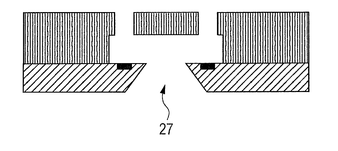
Examples
example 1
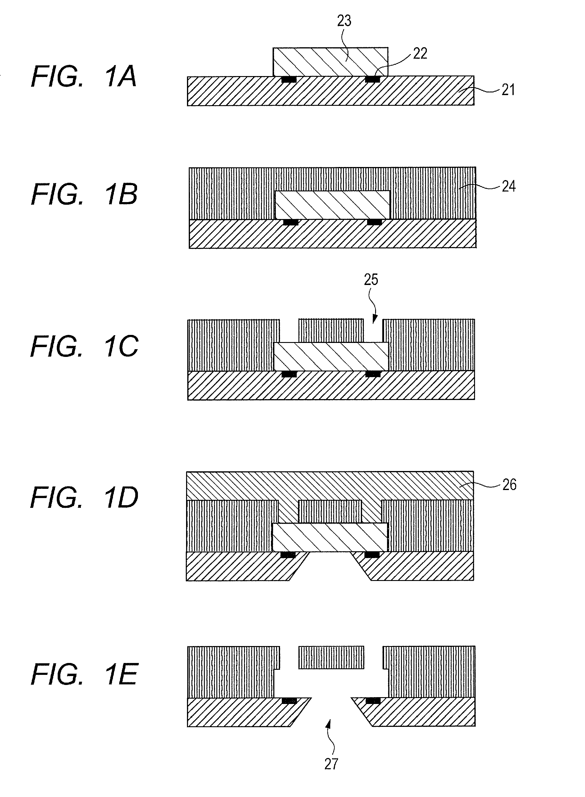
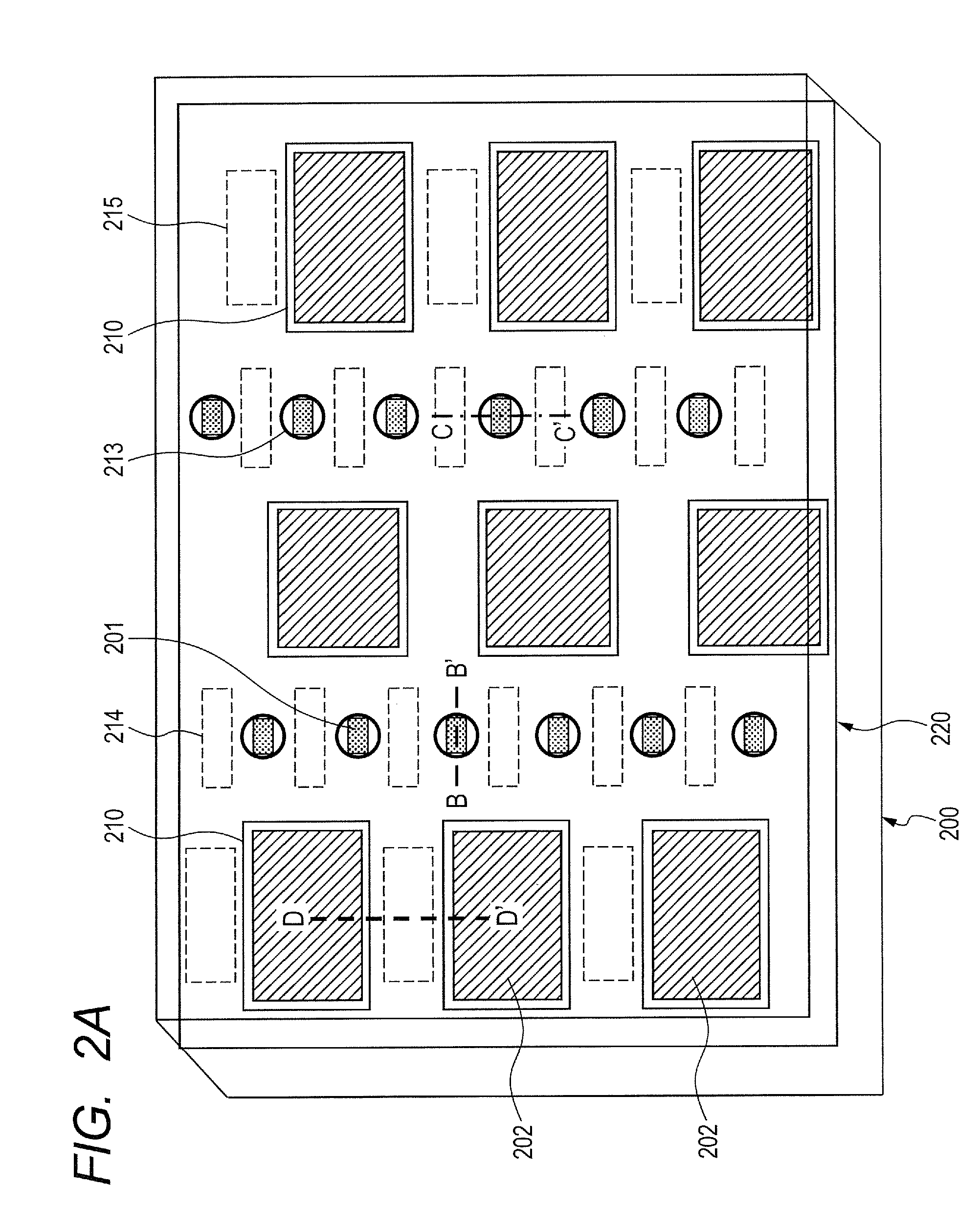
[0082]FIG. 4 is a schematic sectional view of the substrate for the ink jet recording head, in a cross section taken along the dotted line A-A′ illustrated in FIG. 2B.
[0083]The substrate for the ink jet recording head illustrated in FIG. 4 was produced in the following way.
[0084]First, a thermal oxide film 402 (Field-Ox film, hereinafter also referred to as FOx film) was formed on a silicon substrate 401 so as to have a thickness of 1.0 μm, at a temperature of 1,000° C. with a thermal diffusion step (LOCOS: Local Oxidation of Silicon step).
[0085]Next, a BPSG film (film of silicate glass containing boron and phosphorus) 403 was formed on the thermal oxide film 402 so as to have a thickness of 0.6 μm, with the use of a PCVD method.
[0086]Next, a first electric wiring layer 404 formed of an Al film was formed on the BPSG film 403, the thermal oxide film 402 and the silicon substrate 401 so as to have a thickness of 0.4 μm.
[0087]Next, an interlayer insulation film 405 using P—SiO was for...
example 2
[0126]As is disclosed in the steps of producing the ink jet recording head according to the present embodiment in FIGS. 5A to 5G, an independent supply port is formed by dry etching of silicon, after a patterning mask has been formed in a recessed portion (common supply port) which has been formed on the rear face of a silicon substrate. It is known that the formation accuracy of the patterning mask in the recessed portion which has been formed on the rear face of the silicon substrate, and the processing accuracy of the dry etching of silicon in the bottom surface of the recessed portion are slightly inferior compared to the accuracy of processing on the surface of the silicon substrate. Then, FIG. 6 illustrates a schematic sectional view of the substrate for the ink jet recording head, in a cross section taken along the dotted line A-A′ illustrated in FIG. 2B, in which the accuracy on the rear face of the silicon substrate is assumed to occasionally deviate by several μm. In the p...
example 3
[0127]Similarly to that in Example 2, in order to achieve the present invention, FIG. 7 illustrates a schematic sectional view of the substrate for the ink jet recording head, in a cross section taken along the dotted line A-A′ illustrated in FIG. 2B, in which the accuracy on the rear face of the silicon substrate is assumed to occasionally deviate by several μm. In FIG. 7, a side etching stopper portion 711 is arranged on a thermal oxide film 702 and a silicon substrate 701, and a part of the side etching stopper portion 711 contacts the silicon substrate 701. In other words, the ink jet recording head is structured so that the side etching stopper portion 711 is arranged between the thermal oxide film 702 and the etching stop layer. In addition, the etching stop layer and the side etching stopper portion are arranged on the first face of the silicon substrate 710, and the side face of the etching stop layer contacts the side face of the side etching stopper portion. By having such...
PUM
 Abstract
Description
Claims
Application Information
 - R&D Engineer
- R&D Manager
- IP Professional
- Industry Leading Data Capabilities
- Powerful AI technology
- Patent DNA Extraction
Browse by: Latest US Patents, China's latest patents, Technical Efficacy Thesaurus, Application Domain, Technology Topic, Popular Technical Reports.
© 2024 PatSnap. All rights reserved.Legal|Privacy policy|Modern Slavery Act Transparency Statement|Sitemap|About US| Contact US: help@patsnap.com