

Optical Light Guide Element For An Electronic Device
a technology of optical light guide elements and electronic devices, which is applied in the direction of optical radiation measurement, instruments, lighting and heating apparatus, etc., can solve the problems of insufficient space for optical light guide elements, insufficient space for additional components, and inability to meet the needs of mobile electronic devices
Inactive Publication Date: 2013-10-31
HEPTAGON MICRO OPTICS
View PDF7 Cites 16 Cited by
- Summary
- Abstract
- Description
- Claims
- Application Information
AI Technical Summary
Benefits of technology
The patent describes a device that redirects light incident at a steep angle and reduces its loss by reducing the number of reflections. This is achieved by using an inclined surface that causes the light to propagate in a direction towards the second end section. The device also includes an IR blocking filter to reduce sensitivity to infrared content. The optical light guide element is efficient, uniform, and can capture and guide light with an angle of incident from -60° to +60°.
Problems solved by technology
However, mobile electronic devices have to be light and small-sized.
Therefore, the numerous components within the housing of such an electronic device are normally densely packed and space for additional components is often extremely limited.
This means that in such a case there is not a lot of available space for an optical light guide element.
However, light guide elements in the state-of-the-art are known for being bulky and for needing a lot of space.
Method used
View moreImage
Smart ImageViewing Examples

Examples
first embodiment
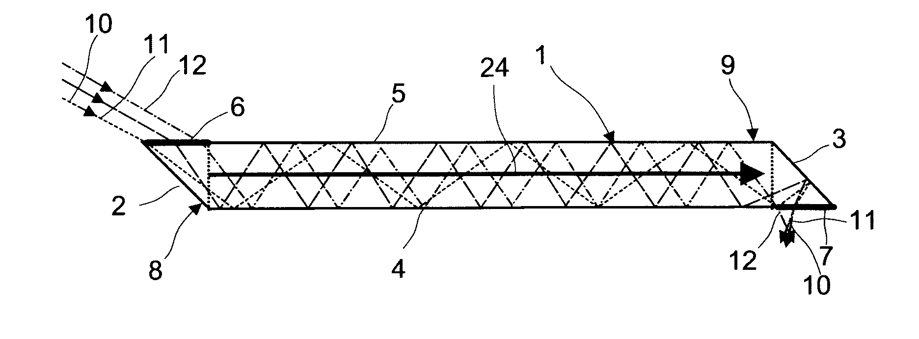
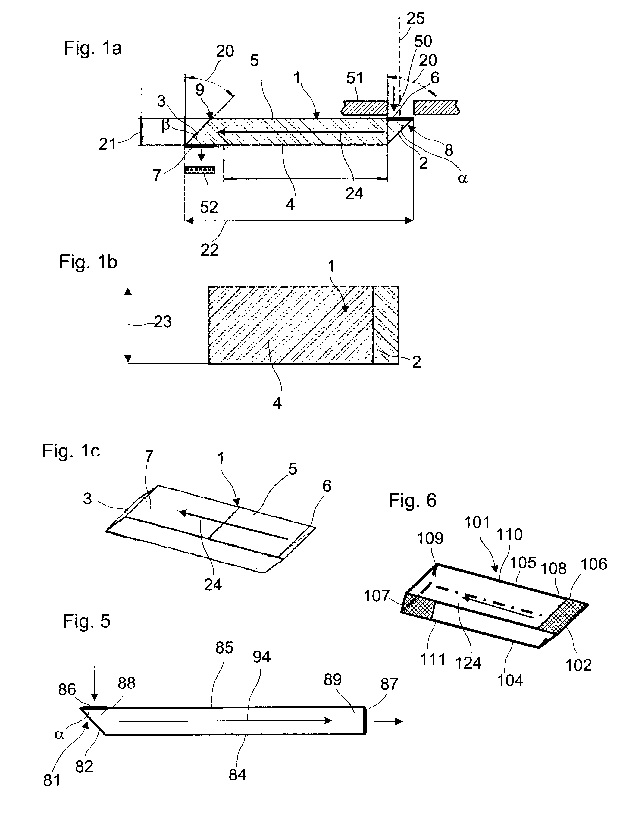
[0045]FIGS. 1a . . . c: show different views of an optical light guide element;
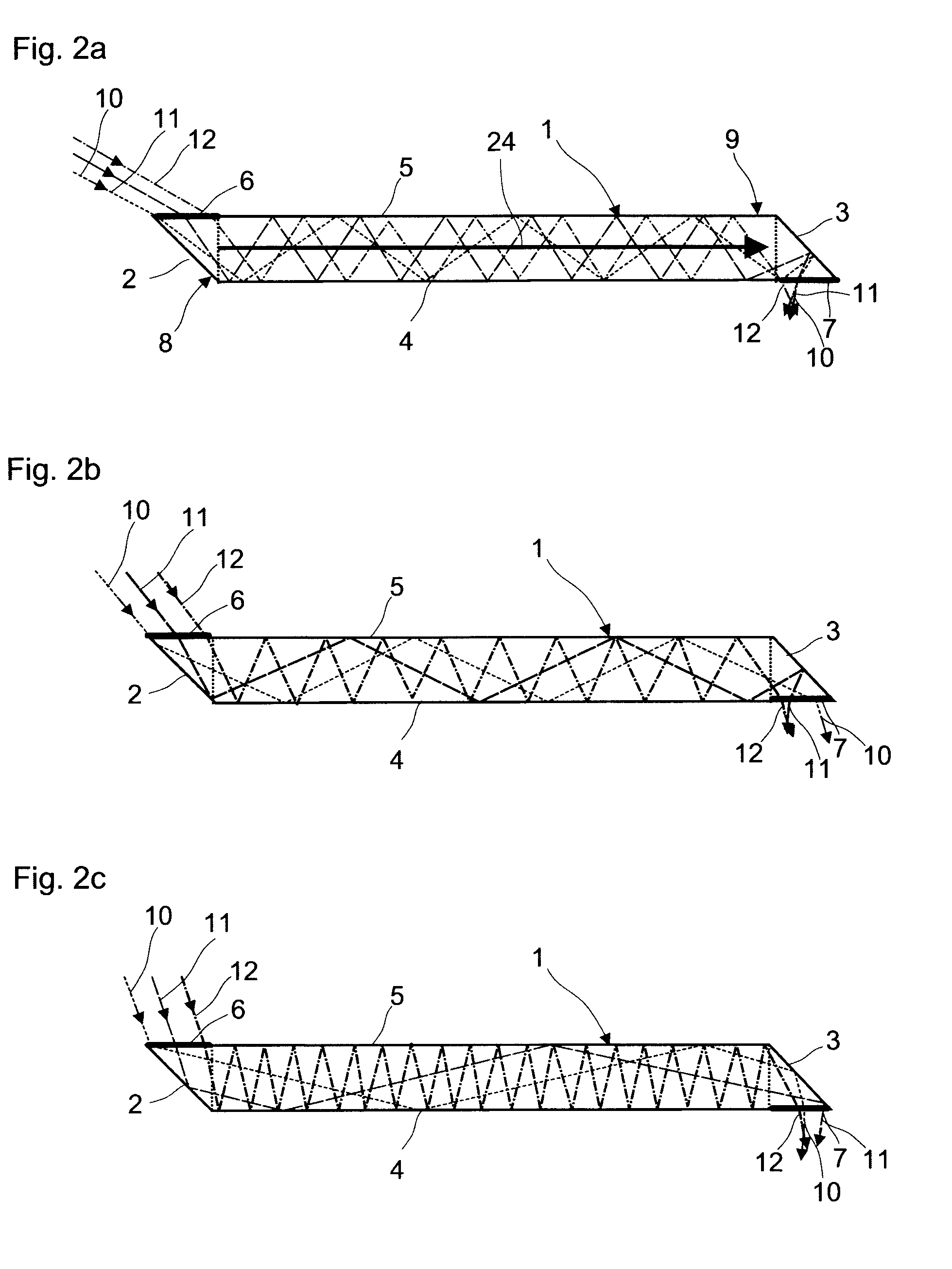
[0046]FIGS. 2a . . . g: show the light path within the optical light guide element according to the first embodiment of light beams which impinge the light entrance area from different angles;
second embodiment
[0047]FIGS. 3a . . . c: show different views of an optical light guide element;
third embodiment
[0048]FIG. 4: shows an optical light guide element;
Login to View More PUM
| Property | Measurement | Unit |
|---|---|---|
| distance | aaaaa | aaaaa |
| distance | aaaaa | aaaaa |
| distance | aaaaa | aaaaa |
Abstract
The invention relates to an optical light guide element (1) having a first end section (8) with a light entrance area (6) designed for facing a light-transparent opening (50) and having a second end section (9) with a light exit area (7) designed for facing a light sensor (52), wherein the light entrance area (6) is defined by a surface area on the optical light guide element (1) which faces the light-transparent opening (50) and the first end section (8) forms an inclined surface area (2) which has an acute angle with the surface area of the light entrance area (6).
Description
FIELD OF THE INVENTION[0001]The invention relates to optical light guide elements for electronic devices and to electronic devices containing optical light guide elements.BACKGROUND OF THE INVENTION[0002]Portable electronic devices, such as mobile phones, multi-function smart phones, digital media players, digital cameras and navigation devices have display screens that can be used under various lighting environments. Such devices have integrated in them a function that can provide (in real-time) an indication of the current level of visible light in the immediate environment outside the device. This is called an ambient light sensor function (or ALS). The ALS can be used for applications such as automatically managing the brightness of a display screen for better readability or for saving battery energy (depending upon the current ambient light level).[0003]On the market ALS integrated circuit (IC) devices are known that have a built-in solid state light sensor together with associ...
Claims
Login to View More Application Information
Patent Timeline
 Patent Type & AuthorityApplications(United States)
IPC IPC(8): F21V8/00
CPCG02B6/0011G02B6/0018G09G2360/144B29D11/00663B29D11/00865G01J1/4204G01J1/0407G02B6/00G06F1/16G06F1/1601G06F1/1626
InventorKETTUNEN, VILLERIEL, PETERRUDMANN, HARTMUTROSSI, MARKUS
OwnerHEPTAGON MICRO OPTICS