Electroconductive sheet and touch panel

a technology of conductive sheets and touch panels, applied in the direction of conductors, instruments, superimposed coating processes, etc., can solve the problems of deteriorating the detection sensitivity of touch positions, the transparent and visible touch panel electrodes of thin metal wires, etc., and achieve the effect of improving detection sensitivity and high transparency

Active Publication Date: 2013-12-12
FUJIFILM CORP
View PDF2 Cites 74 Cited by
  • Summary
  • Abstract
  • Description
  • Claims
  • Application Information

AI Technical Summary

Benefits of technology

[0036]As described above, the conductive sheet and the touch panel of the present invention can have the electrodes

Problems solved by technology

The touch panel electrode of the thin metal wires has problems with transparency and visibility because the thin metal wires are composed of an opaque material.
However, the el

Method used


Image

  • Electroconductive sheet and touch panel
  • Electroconductive sheet and touch panel
  • Electroconductive sheet and touch panel

Examples


examples

[0248]The present invention will be described more specifically below with reference to Examples. Materials, amounts, ratios, treatment contents, treatment procedures, and the like, used in Examples, may be appropriately changed without departing from the scope of the present invention.

[0249]The following specific examples are therefore to be considered in all respects as illustrative and not restrictive.

first example

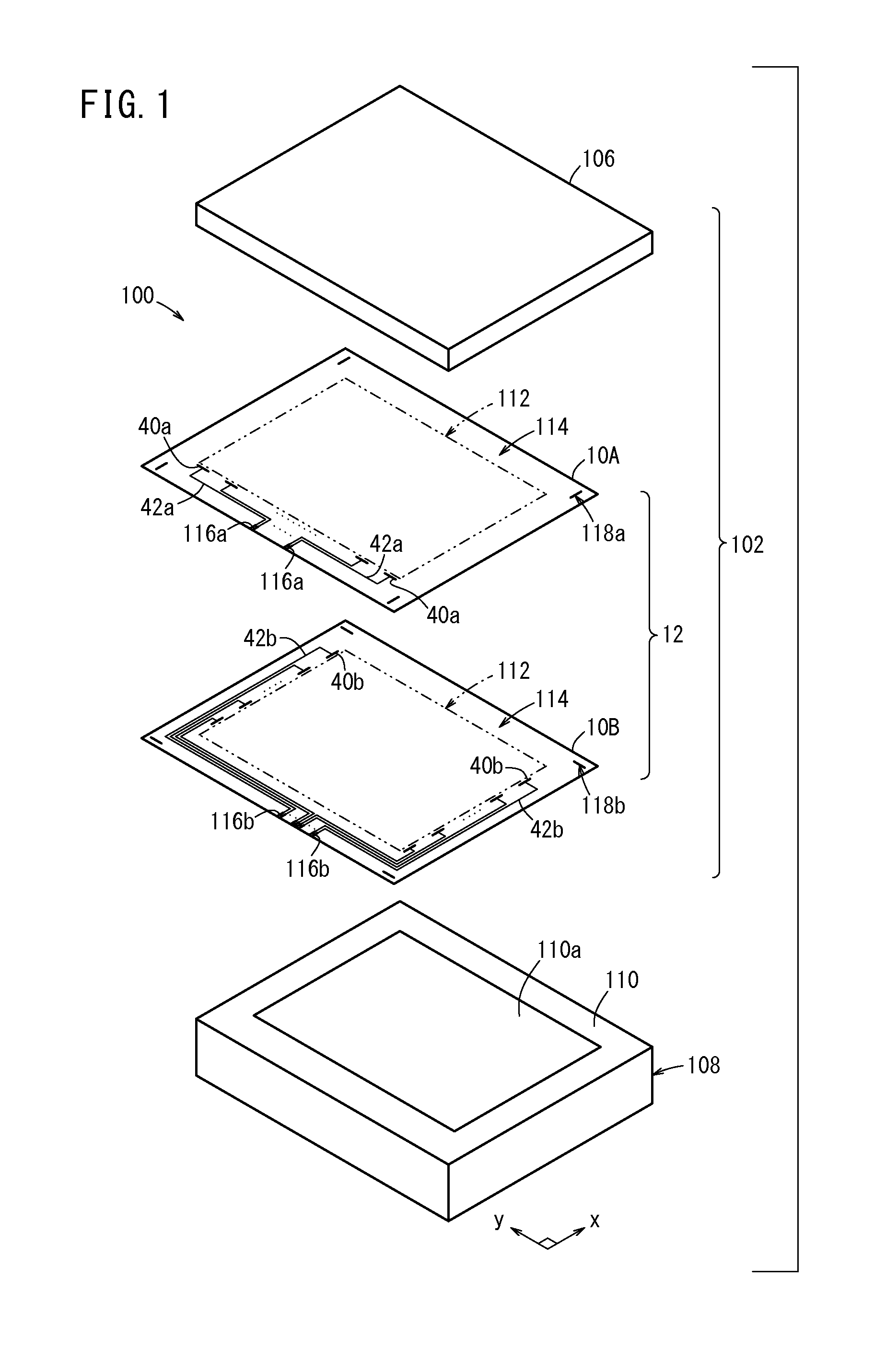
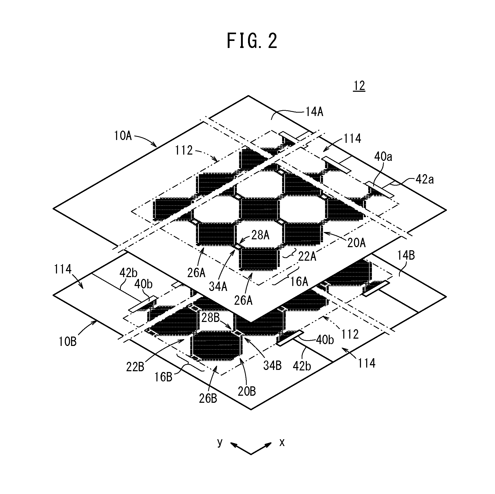
[0250]In First Example, in Examples 1 to 9 and Comparative Examples 1 and 2, the ratio (A2 / A1) of the occupation area A2 of the thin metal wires 15 in the second conductive patterns 26B to the occupation area A1 of the thin metal wires 15 in the first conductive patterns 26A and the ratio (a2 / a1) of the occupation area a2 of the thin metal wires 15 in the second large lattices 16B to the occupation area a1 of the thin metal wires 15 in the first large lattices 16A were changed to evaluate the surface resistances of the first conductive patterns 26A and the second conductive patterns 26B and the detection sensitivity of the conductive sheet stack 12. The properties and evaluation results of Examples 1 to 9 and Comparative Examples 1 and 2 are shown in Table 3.

example 1

[0259]The first conductive sheet 10A and the second conductive sheet 10B of Example 1 were produced in the above manner. Both of the occupation area ratios A2 / A1 and a2 / a1 were 2.


PUM

PropertyMeasurementUnit
Thicknessaaaaaaaaaa
Thicknessaaaaaaaaaa
Lengthaaaaaaaaaa

Abstract

An electroconductive sheet and a touch panel having a first electroconductive section and a second electroconductive section, the second electroconductive section being disposed on the display-panel side. The first electroconductive section has a plurality of first electroconductive patterns arranged in the x-direction, a plurality of first large grids being respectively connected to the first electroconductive patterns. The second electroconductive section has a plurality of second electroconductive patterns arranged in the y-direction, a plurality of second large grids being respectively connected to the second electroconductive patterns. The area occupied by thin metal wires in the second electroconductive patterns is larger than the area occupied by thin metal wires in the first electroconductive patterns. The area occupied by thin metal wires in the second large grids is larger than the area occupied by thin metal wires in the first large grids.

Description

CROSS-REFERENCE TO RELATED APPLICATIONS AND PRIORITY CLAIMS[0001]This application is a Continuation of International Application No. PCT / JP2012 / 054097 filed on Feb. 21, 2012, which was published under PCT Article 21(2) in Japanese, which is based upon and claims the benefit of priority from Japanese Patent Application No. 2011-038703 filed on Feb. 24, 2011, the contents all of which are incorporated herein by reference.TECHNICAL FIELD[0002]The present invention relates to a conductive sheet and a touch panel, for example suitable for use in a projected capacitive touch panel.BACKGROUND ART[0003]Transparent conductive films containing thin metal wires have been studied as disclosed in US Patent Application Publication No. 2004 / 0229028, International Publication No. 2006 / 001461, etc.[0004]Touch panels have attracted much attention in recent years. Though the touch panels has currently been used mainly in small devices such as PDAs (personal digital assistants) and mobile phones, it is...

Claims


Application Information

Patent Timeline
IPC IPC(8): H01B5/00
CPCH01B5/00G06F2203/04111G06F2203/04112G06F3/0445G06F3/0446
Inventor ICHIKI, AKIRA
Owner FUJIFILM CORP
Why Eureka
Try Eureka