Minute structure and information recording medium

a technology of information recording medium and minute structure, which is applied in the direction of instruments, non-metal conductors, lighting and heating apparatus, etc., can solve the problems of high cost, unsuitable for simple circuit design, and high production cost, and achieve the effect of low cos

Inactive Publication Date: 2014-01-30
RICOH KK
View PDF4 Cites 11 Cited by
  • Summary
  • Abstract
  • Description
  • Claims
  • Application Information

AI Technical Summary

Benefits of technology

[0022]According to one aspect of the invention, there is disclosed a minute structure which can be easily formed by using the heat lithography.
[0023]According to one aspect of the invention, there is disclosed a minute-structure manufacturing method which can easily form a minute structure by using the heat lithography.
[0024]According to one aspect of the invention, there is disclosed a write-once information recording medium which can be produced with low cost and can form a minute recording mark therein.
[0045]According to the embodiments of the invention, it is possible to provide a minute structure which can be easily formed by using the heat lithography, and a minute-structure manufacturing method which can easily form a minute structure by using the heat lithography.
[0047]According to the embodiments of the invention, it is possible to provide a write-once information recording medium which can be produced with low cost and can form a minute recording mark therein.

Problems solved by technology

However, these exposure systems require the vacuum source and they are expensive, and the production cost becomes high.
Since the existing method requires an expensive electron-beam lithography system, it has a problem of high cost.
However, it is unsuitable for a simple circuit design at a time of specification change and a simple experiment at an experimental stage.
However, the production needs much time and the material used is limited to the resin that can be produced by a photopolymerization reaction.
There is also a problem that, when forming a concave part in the second dielectric layer, the end of the concave part is roughed.

Method used


Image

  • Minute structure and information recording medium
  • Minute structure and information recording medium
  • Minute structure and information recording medium

Examples


embodiment 1

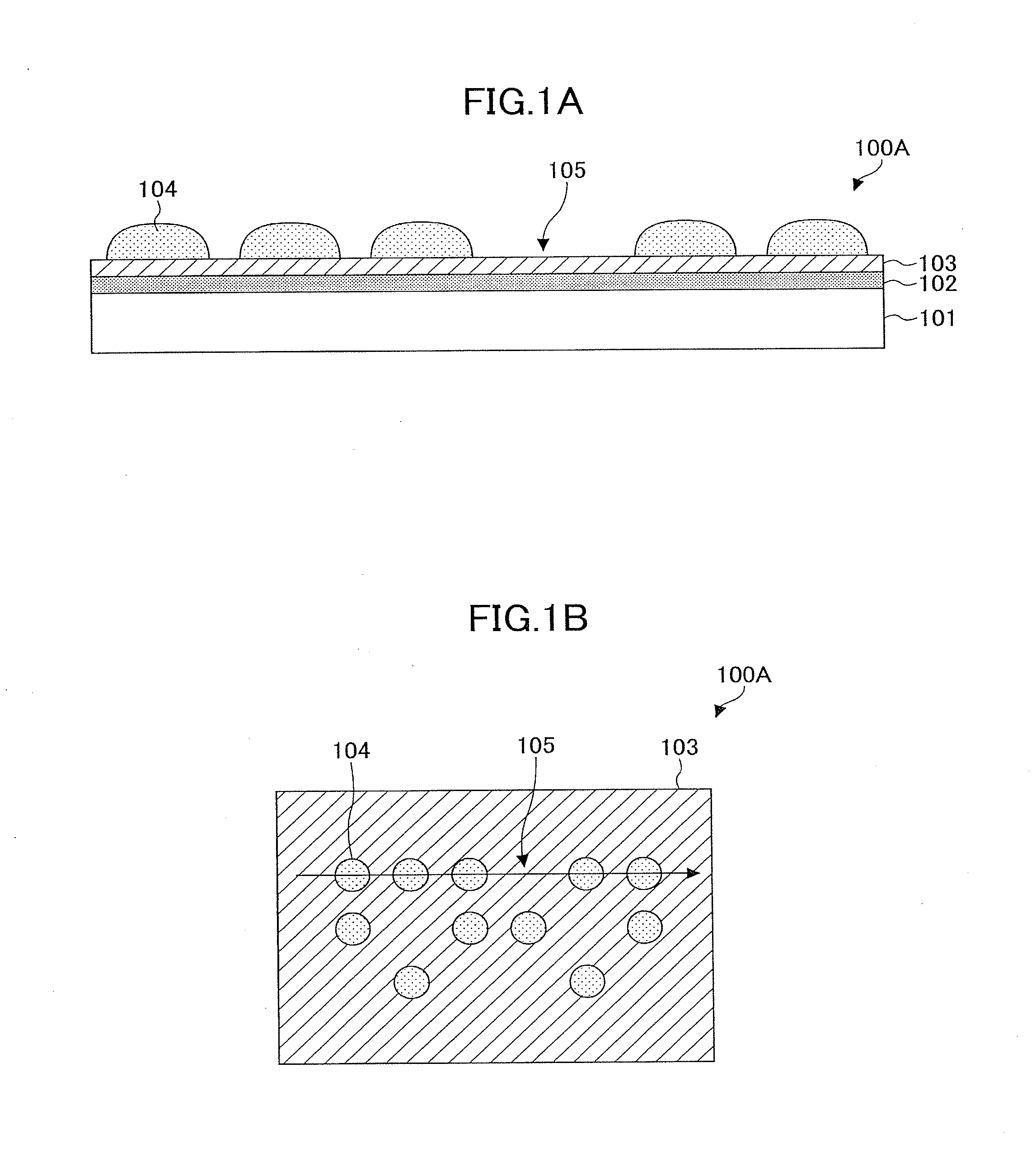
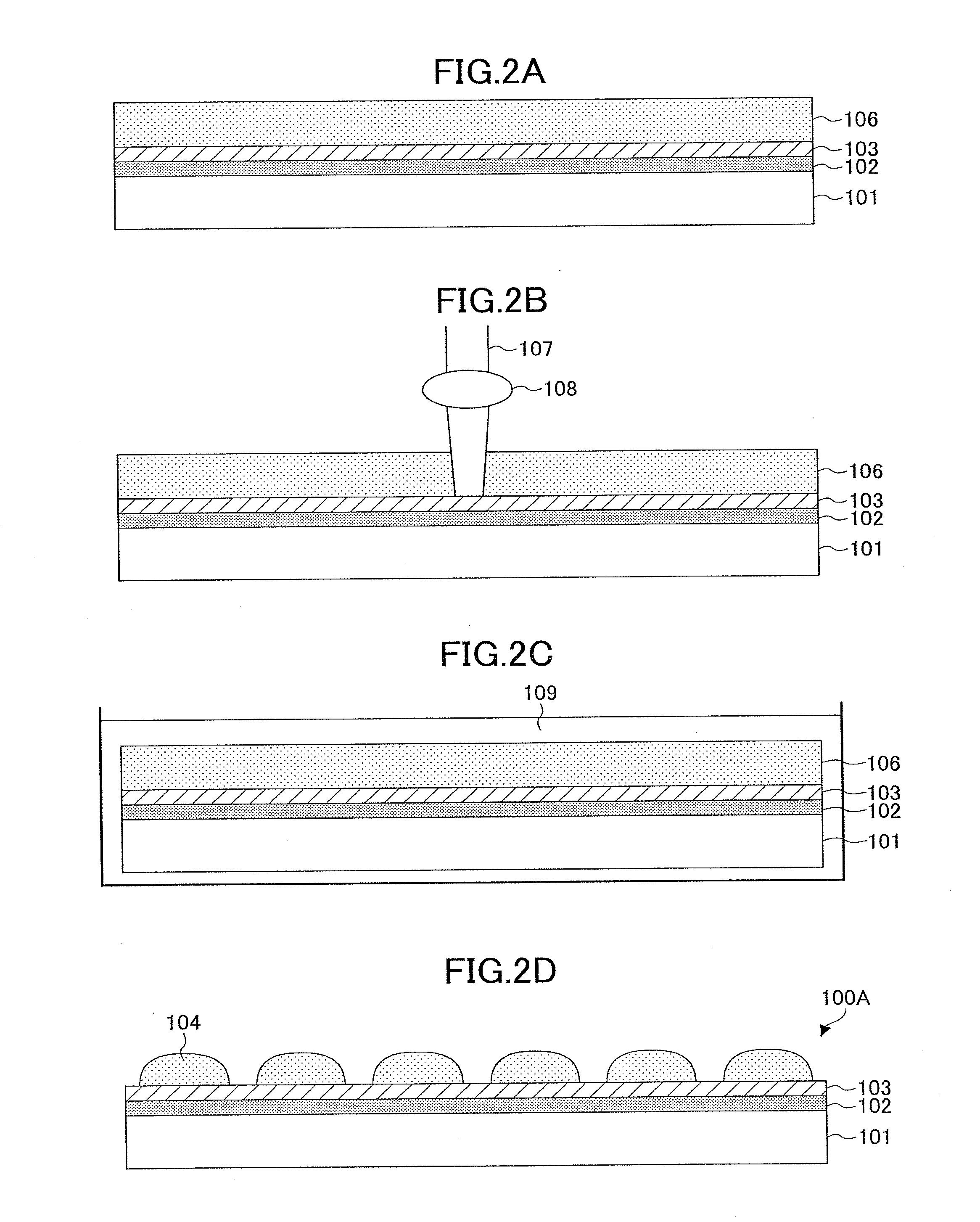
[0149]FIG. 1A and FIG. 1B show the composition of an information recording medium 100A of the embodiment 1 of the invention. FIG. 1A is a cross-sectional view of the information recording medium and FIG. 1B is a top view of the information recording medium.

[0150]In the information recording medium 100A, a 50 nm-thick dielectric layer 102 of ZnS—SiO2 (the molar ratio: 8:2), a 10 nm-thick light absorption layer 103 of AgInSbTe, and minute structures 104 are formed on a silicon substrate 101 with a thickness of 1 mm and a size of 10 cm by 10 cm.

[0151]The minute structures 104 are arranged as shown in FIG. 1B, and information is determined by the existence of minute structure 104. Specifically, when the recording medium 100A is irradiated by a laser beam, a fluorescent light is emitted by the minute structure 104, and no fluorescent is emitted from the area 105 where no minute structure 104 is arranged, so that this recording medium 100A may function as an information recording medium.

[...

embodiment 2

[0158]FIG. 3A and FIG. 3B show the composition of an information recording medium 100B of the embodiment 2 of the invention. FIG. 3A is a cross-sectional view of the information recording medium and FIG. 3B is a top view of the information recording medium.

[0159]In the information recording medium 100B, a 50 nm-thick dielectric layer 102 of ZnS—SiO2 (the molar ratio: 8:2), a 10 nm-thick light absorption layer 103 of Ge (germanium), a 20 nm-thick ZnS layer 111, and minute structures 104 are formed on a polycarbonate substrate 110. The polycarbonate substrate 110 is a disc-like plate for optical disk with a diameter of 12 cm and a height of 20 nm, and it has lands and grooves in a period of 440 nm (track pitch).

[0160]The minute structures 104 are arranged as shown in FIG. 3B, and information is determined by the existence of minute structure 104. Specifically, when the recording medium 100B is irradiated by a laser beam, a fluorescent light is emitted from the minute structure 104, an...

embodiment 3

[0168]The pulsed light output dependency of the minute structure was investigated. The pulsed light output was varied in a range of 1.5-7 mW. The method of manufacturing the minute structure was the same as that of the embodiment 2. As the material of minute structure, ZnS—SiO2 (the molar ratio: 8:2) was used.

[0169]FIG. 4A through FIG. 9B show the scanning electron microscope photographs of the produced minute structures. The observation is performed using a field-emission scanning electron microscope FE-SEM 5-4100 (from Hitachi Ltd.).

[0170]In FIG. 4A through FIG. 9B, both the SEM photographs taken from the top surface direction and the SEM photographs taken from the slanting direction are shown. As is apparent from these SEM photographs, the configuration of minute structure including the height and the width is varied in accordance with a change of the pulsed light output.

[0171]In the embodiment 3, even when the minute structure is formed in any of the shown configurations, it can...


PUM

PropertyMeasurementUnit
optical absorption abilityaaaaaaaaaa
semiconductoraaaaaaaaaa
thicknessaaaaaaaaaa

Abstract

There is disclosed a minute structure including a sulfur compound and a silicon oxide. There is also disclosed a write-once information recording medium including a substrate and a recording layer formed of a mixed inorganic material and deposited on the substrate, wherein the mixed inorganic material contains a sulfur compound and a silicon oxide.

Description

BACKGROUND OF THE INVENTION[0001]1. Field of the Invention[0002]This invention relates to a minute structure and a write-once (WORM, or write-once read-many) information recording medium.[0003]2. Description of the Related Art[0004]Recently, the research and development of minute structures with a size ranging from nanometer scale to micrometer scale is carried out in many fields including nanophotonics, high-density recording media, optical elements, and biochemical chips. What is indispensable to those devices utilizing the opto-electronics is a material which is optically transparent in a visible light region and has little optical loss. For this reason, the research and development of a technology for producing a minute structure from a transparent material is carried out briskly.[0005]Zinc oxide is optically transparent in a visible light region and has a property to absorb ultraviolet light. Zinc oxide is used for the purposes, such as LED, transparent transistor, UV cut mater...

Claims


Application Information

Patent Timeline
Patent Type & Authority Applications(United States)
IPC IPC(8): G11B7/26G11B7/243G11B7/2403G11B7/24085G11B7/246G11B7/2467
CPCG11B7/243G11B7/26B82Y10/00B82Y30/00G11B7/00452G11B7/2403G11B7/24085G11B7/2467G11B7/261G11B7/263G11B2007/24312G11B2007/2432G11B2007/24324
Inventor MORI, TETSUJI
Owner RICOH KK
Why Eureka
Try Eureka