Wiring board
a wiring board and wire technology, applied in the field of wiring boards, can solve the problems of inability to apply known design methods in practice, inability to avoid intra skew and impedance mismatch according to the conventional design, and difficulty in adjusting the width of the wiring and the thickness of the wiring in manufacturing, etc., to achieve excellent transmission properties and solve impedance mismatch.
- Summary
- Abstract
- Description
- Claims
- Application Information
AI Technical Summary
Benefits of technology
Problems solved by technology
Method used
Image
Examples
first embodiment
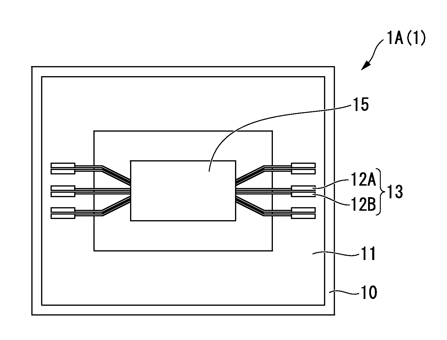
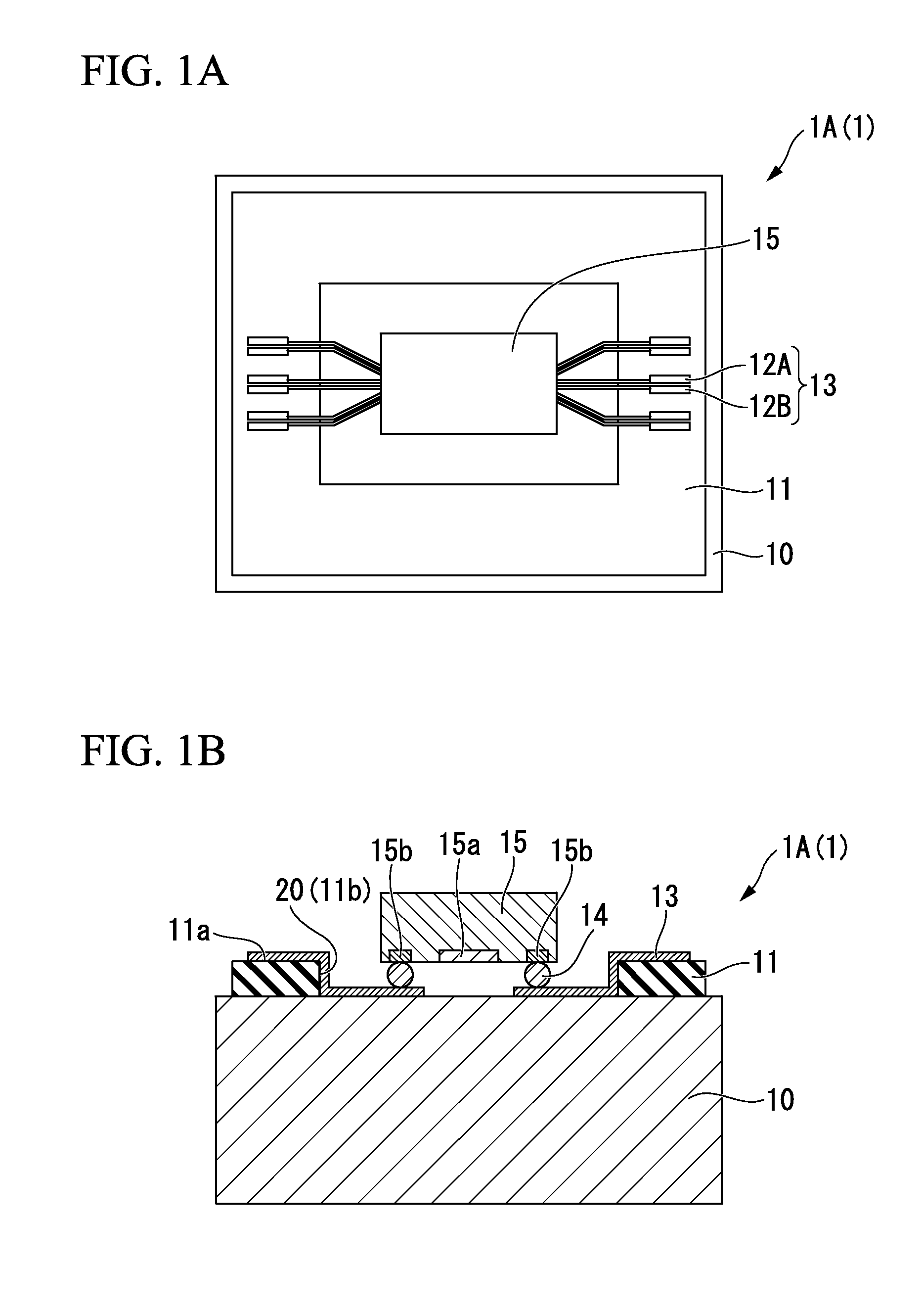
[0047]FIGS. 1A and 1B is a view showing an exemplary configuration of a wiring 1 board according to the first embodiment of the present invention, in which FIG. 1A is a plan view while FIG. 1B is a cross-sectional view.
[0048]A wiring board 1A (1) according to the present embodiment includes a differential transmission line 13 constituted by two wirings 12A and 12B which are disposed on a face 10a of a board 10 to be parallel to each other.
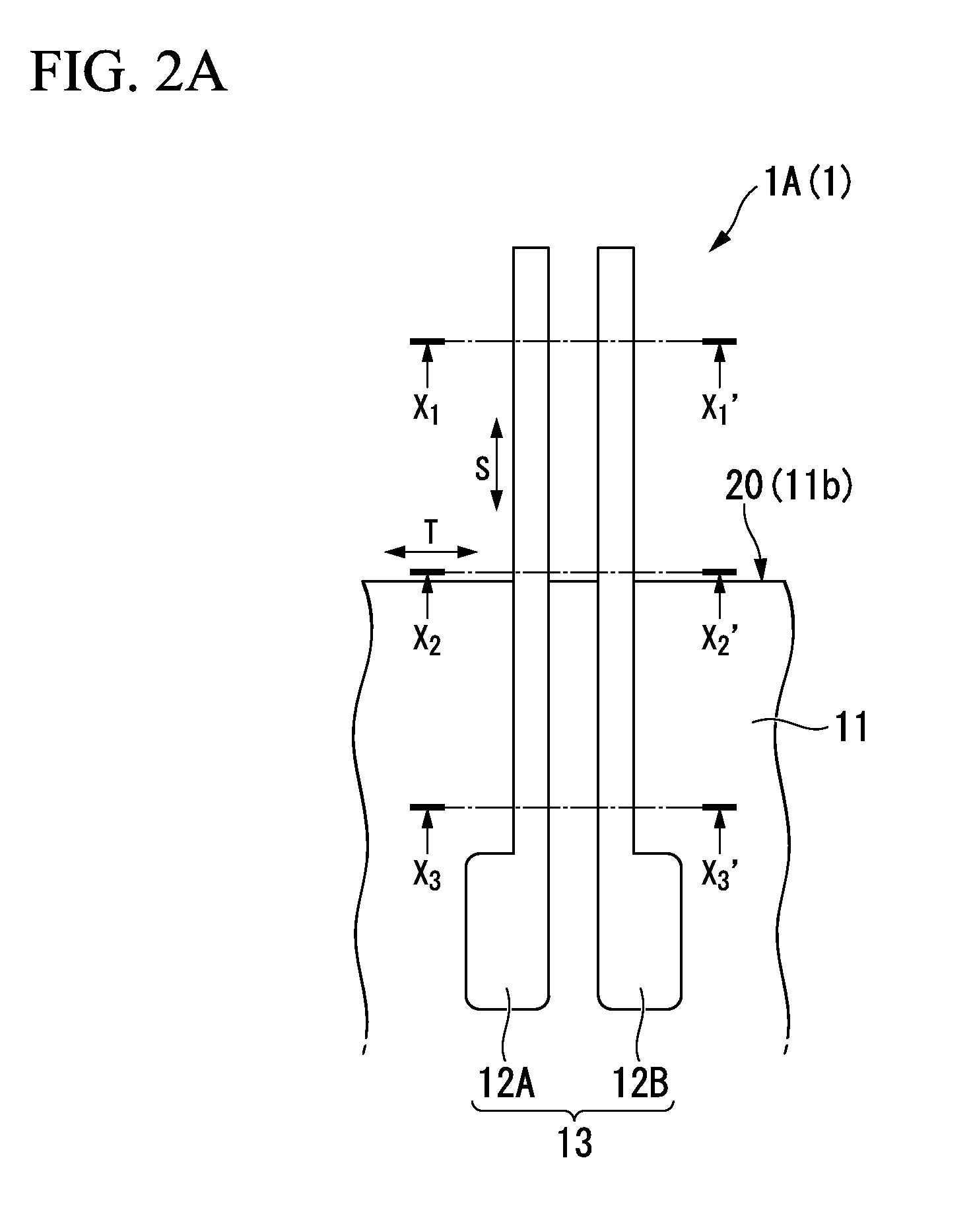
[0049]The wiring board 1A (1) includes an insulation resin layer 11(insulation layer) formed in part of the face 10a of the board 10. At the boundary between the face 10a of the board 10 and a top face 11a of the insulation resin layer 11, a stepped portion 20 is formed which is constituted by a lateral face 11b of the insulation resin layer 11. The two wirings 12A and 12B constituting the differential transmission line 13 extend from the face 10a of the board 10 to the top face 11a of the insulation resin layer 11 so as to traverse the stepped por...
second embodiment
[0071]Hereinafter, a wiring board 1 according to the second embodiment of the present invention will be explained.
[0072]It should be noted that components different from that of the above-described first embodiment will be mainly explained below and explanations of the same components as that of the first embodiment will be omitted.
[0073]FIGS. 4A and 4B are a view showing an exemplary configuration of the wiring board according to the present embodiment, and particularly is an enlarged perspective view showing a differential transmission line.
[0074]In the above-described first embodiment, as shown in FIG. 4A, the lateral face 11b of the insulation resin layer 11 constituting the stepped portion 20 is substantially perpendicular to the face 10a of the board 10.
[0075]In contrast, in a wiring board 1D (1) according to the present embodiment (second embodiment), as show in FIG. 4B, the lateral face 11b of the insulation resin layer 11 constituting the stepped portion 20 is oblique to th...
third embodiment
[0077]Hereinafter, a wiring board 1 according to the third embodiment of the present invention will be explained.
[0078]It should be noted that components different from that of the above-described first embodiment will be mainly explained below and explanations of the same components as that of the first embodiment will be omitted.
[0079]FIG. 5-FIG. 8 are a view showing an exemplary configuration of the wiring board according to the present embodiment, and particularly is an enlarged perspective view showing a differential transmission line.
[0080]In a wiring board 1E (1) shown in FIG. 5, the width of the two wirings 12A and 12B in the top face 11a of the insulation resin layer 11 varies such that the respective widths of the two wirings 12A and 12B are the same as each other at each position equidistant from the periphery (11b).
[0081]In the wiring board 1E (1) according to the present embodiment, since the width of the two wirings 12A and 12B in the top face 11a of the insulation res...
PUM
 Abstract
Description
Claims
Application Information


