
Display device for decompressing compressed image data received

a display device and image data technology, applied in the field of display devices, can solve the problems of increasing scanning frequency, insufficient time to apply data in each subpixel, and difficulty in coping with the increase in display frequency to display a picture with higher definition, so as to improve the processing performance of the data processor circuit, improve the transfer performance, and avoid the effect of increasing the cos

Inactive Publication Date: 2005-06-21
PANASONIC LIQUID CRYSTAL DISPLAY CO LTD +1
View PDF2 Cites 78 Cited by
  • Summary
  • Abstract
  • Description
  • Claims
  • Application Information

AI Technical Summary

Benefits of technology

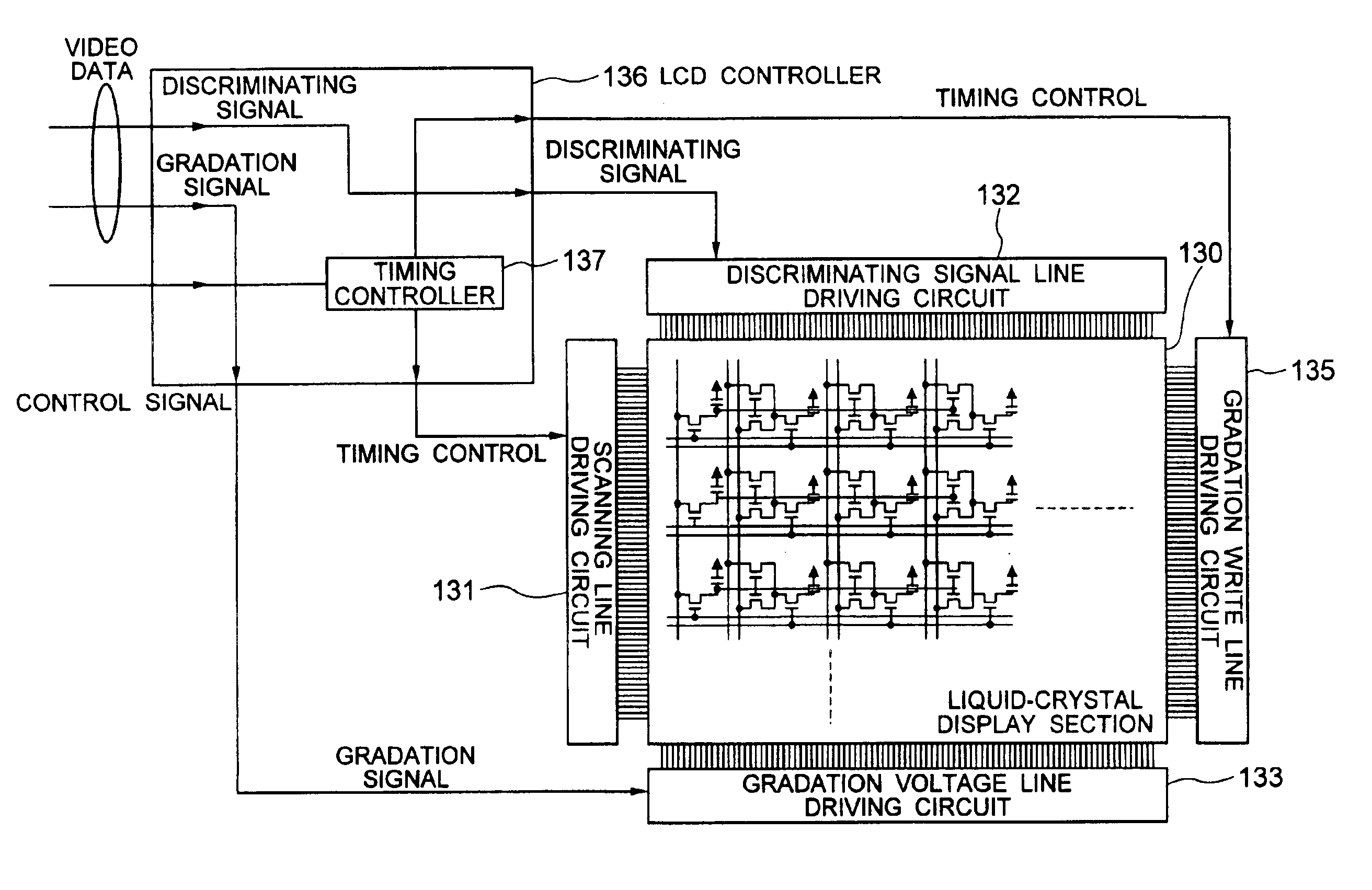
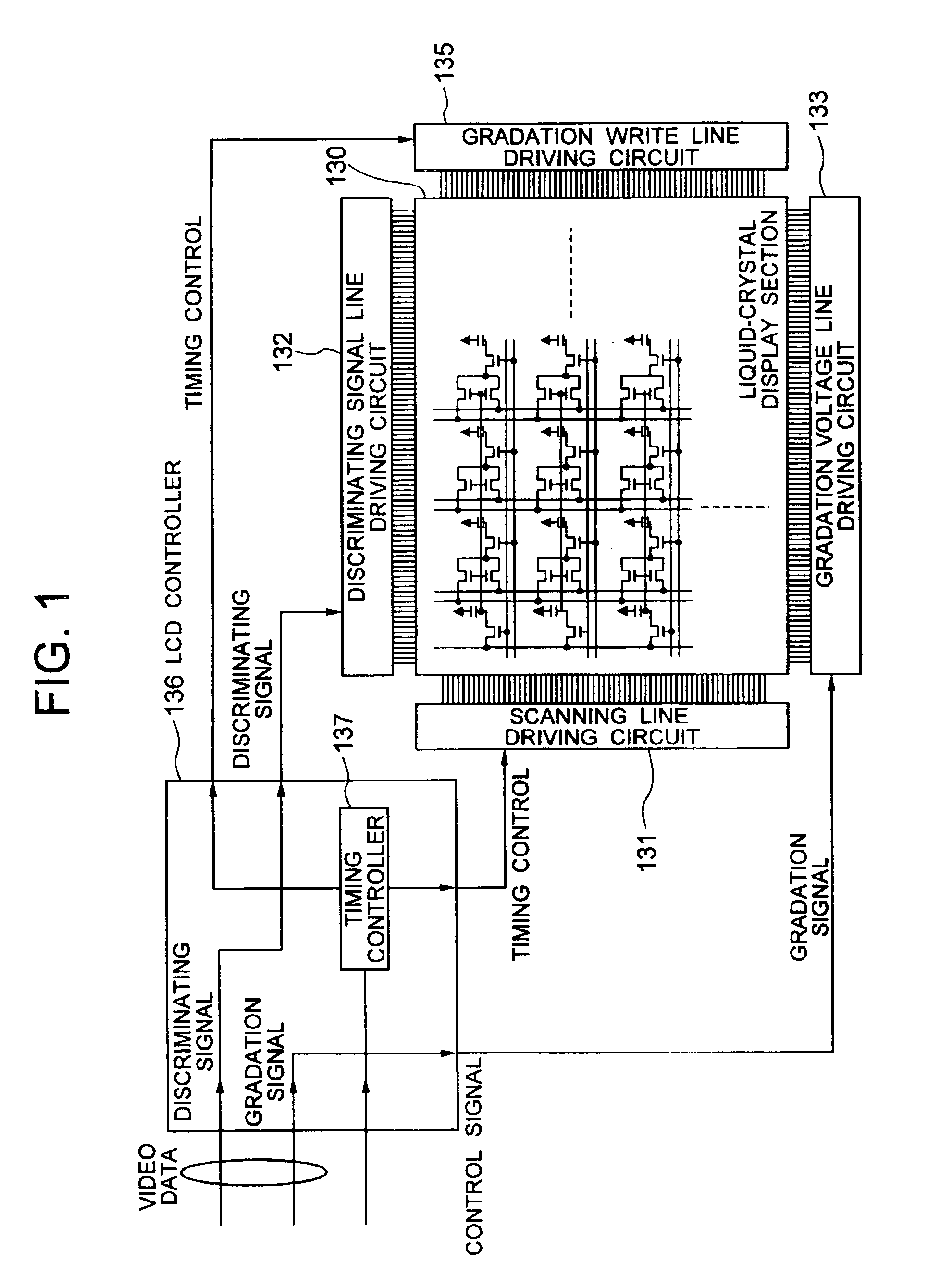
[0017]It is therefore a first object of the present invention to provide display device in which (1) display data with substantially improved transfer performance using the digital PV link method or the image compression method is received, (2) the processing performance of the data processor is only slightly improved and hence the cost is not increased, and (3) a large amount of information can be normally displayed.
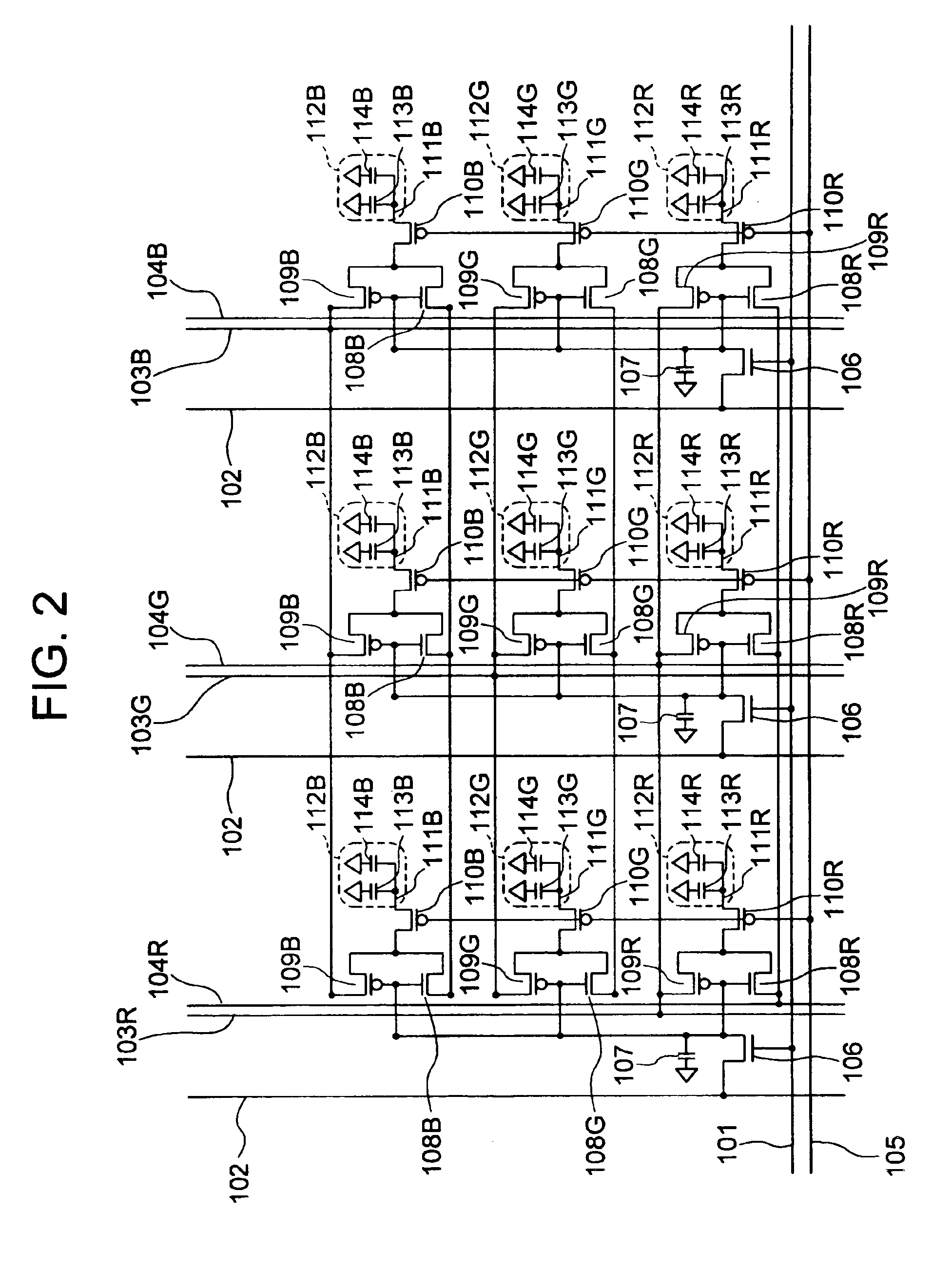
[0018]A second object of the present invention is to provide display device in which to expand a compressed image in the display device, the wiring and active elements are increased and the aperture ratio is reduced, and hence there exists a fear of reduction in brightness; however, the reduction in the aperture ratio is compensated to improve the brightness.
[0021]As a result, the display device can expand the compressed image with a high aperture ratio to display the expanded image.
[0026]According to the present invention, display data with substantially improved transfer performance using the digital PV link method or the image compression method associated with a spatial axis, a gradation axis, and a time axis is received; the processing performance of the data processor circuit is only slightly improved, and hence the cost is not increased and a large amount of information can be normally displayed.

Problems solved by technology

In other words, the image display methods and the image display driving methods of the background art are attended with delay of signals on interconnection lines, insufficient time to apply data in each subpixel, increase in the scanning frequency, and the like.
Therefore, it is difficult to cope with the increase in the display frequency to display a picture with higher definition.
Therefore, this causes blur in the motion picture to resultantly reduce the picture quality.
However, the display frequency is approaching its upper limit in the image display method and the image display driving methods at the present stage of the technique as already described above.
However, during the motion picture display operation in which the overall screen is re-written, high-speed display of a motion picture is difficult due to the delay of signals on the interconnection line and the restricted performance of data writing operation.
In short, because of the increase in the number of pixels and the increase in the frequency to cope with the high definition display and the high-speed display, the image processing in the image controller and the data transmission between the image controller and the image display device become difficult.
However, when a display device of the background art receives data in the PV link method or the image compression method, the display device cannot directly display the received image data.
Therefore, the second problem must be solved, namely, the increase in processing performance of a data processor in the display device must be achieved.
Moreover, since nothing has been conducted for item (3), the image cannot be normally displayed.
Increase in the processing circuit considerably increases the cost.
However, a display method of displaying an image using an image compression method has not been discussed at all.

Method used


Image

  • Display device for decompressing compressed image data received
  • Display device for decompressing compressed image data received
  • Display device for decompressing compressed image data received

Examples


embodiment 1

[0045]Referring now to FIG. 3, description will be given of a layout of display data which is received by the embodiment of a display device and which has substantially improved transfer performance.

[0046]Image data is usually represented as a set of pixels including gradation data for each color. For example, in an image format commonly used for a personal computer or the like, each pixel data is divided into three primary colors of light, namely, red (R), green (G), and blue (B). For each color, 256 gradation levels are indicated by eight bits. In this case, the amount of image information of one pixel is obtained as “8 bits×3 (colors)=24 bits”. Image data of one screen represented by a set of data items of the pixels is called “bit map”. In an image output source such as a personal computer, the bit map is stored in a memory. In an image output method of the background art, data items in a range from an upper-left corner of the bit map to a lower-right corner thereof are outputte...

embodiment 2

[0063]The second embodiment is substantially equal in structure to the first embodiment excepting features described below.

[0064]FIG. 5 shows a subpixel of the embodiment of the display in a circuit diagram. In the second embodiment, the configuration is substantially the same as that of the first embodiment up to the fourth active element 110. However, a light modulating element 112 of the second embodiment is a light modulating element using a light emitting diode (LED) and includes a capacitor 113, a fifth active element 115 including a subpixel electrode 111 as a gate terminal, and an LED element 116 connected via the fifth active element 115 to a current source. The gradation voltage written in the subpixel electrode 111 is simultaneously written also in the capacitor 113. The voltage drives the fifth active element 115 to control a current flowing through the LED element 116 to resultantly modulate a quantity of emitted light. In this way, when an LED light modulating element ...

embodiment 3

[0067]The third embodiment is substantially equal in structure to the first embodiment excepting features described below.

[0068]FIG. 6 shows a subpixel of the embodiment of the display in a circuit diagram. While two gradation voltage lines 1 and 2 are connected to each subpixel in the first embodiment, only one gradation voltage line is connected to each subpixel in this embodiment. Since the second embodiment includes only a second active element corresponding to the n-type active element 108 and does not include any element as a p-type active element, all active elements in the pixels are unipolar elements. Therefore, the active elements can be produced only in a unipolar production process or can be produced in a production method only applicable to unipolar active elements. In either case, the production cost can be reduced.

[0069]Since only one gradation signal line is used in this embodiment, the gradation voltage can be written in pixels of one gradation level in one block by...


PUM

PropertyMeasurementUnit
colorsaaaaaaaaaa
voltageaaaaaaaaaa
gradation voltageaaaaaaaaaa

Abstract

A display device including a plurality of blocks of pixels each of which includes a red subpixel, a green subpixel, and a blue subpixel, each of the blocks including pixels in a form of a matrix having N rows and M columns includes a first active element shared among three subpixels of each pixel and a second active element connected to a second active element formed in each subpixel connected to the first active element. Ma gradation voltage lines (Ma is an integer; M≧Ma≧2) respectively of red, green, and blue subpixels in a direction of the column are commonly connected. The display device directly displays a compressed image signal without developing the image signal into a bit map in which each subpixel has gradation information.

Description

BACKGROUND OF THE INVENTION[0001]The present invention relates to a display device, and in particular, to a display device having a high frequency driving device suitable to display motion pictures with super high definition.[0002]Thickness and weight of picture display devices have been decreased these days, and flat-panel displays (FPD) such as a liquid-crystal display, a plasma display panel (PDP), an electroluminescent (EL) display, and the like have been widely employed in place of a cathode-ray tube (CRT) primarily used as the picture display device. Techniques for a field emission display (FED) and the like are also rapidly being developed. Since personal computers, digital versatile discs, and digital broadcasting are broadly developed, it is required to display super high definition high-speed motion pictures. Requirement for higher performance of the picture display device, particularly, requirement for higher definition and speed of pictures will be needed also in future....

Claims


Application Information

Patent Timeline
Patent Type & Authority Patents(United States)
IPC IPC(8): G09G3/36G02F1/1368G02F1/133G09G3/20
CPCG09G3/3607G09G3/3659G09G2340/02G09G2300/0842G09G2300/0809
Inventor HIYAMA, IKUOYAMAMOTO, TSUNENORIKONNO, AKITOYOTSUMURA, MAKOTO
Owner PANASONIC LIQUID CRYSTAL DISPLAY CO LTD
Learn More