
Programmable memory built in self repair circuit

a self-repair circuit and programmable memory technology, applied in the direction of information storage, static storage, digital storage, etc., can solve the problems of increasing complexity and density of memories, new failure modes, and becoming increasingly critical

Active Publication Date: 2014-03-20
MOSYS INC
View PDF3 Cites 63 Cited by
  • Summary
  • Abstract
  • Description
  • Claims
  • Application Information

AI Technical Summary

Benefits of technology

The patent describes an integrated circuit chip that has a built-in self-repair feature. This feature receives signals from outside the chip and uses a programmable engine to fix any defects that may occur. The chip also includes a cache to remember which parts are defective. Overall, this feature improves the reliability and efficiency of the integrated circuit.

Problems solved by technology

Testing memories in a chip has become increasingly critical as memories have increased in complexity and density.
The shrinking of geometries has even grater effect upon memories due to their tight layout hence creating new failure modes.
High speed testers are expensive and they need dedicated access to the memories.

Method used


Image

  • Programmable memory built in self repair circuit
  • Programmable memory built in self repair circuit
  • Programmable memory built in self repair circuit

Examples


Embodiment Construction

[0013]Reference will now be made in detail to various embodiments, examples of which are illustrated in the accompanying drawings. While the subject matter will be described in conjunction with these embodiments, it will be understood that they are not intended to limit the subject matter to these embodiments. Furthermore, in the following description, numerous specific details are set forth in order to provide a thorough understanding of the subject matter. In other instances, conventional methods, procedures, objects, and circuits have not been described in detail as not to unnecessarily obscure aspects of the subject matter.

Notation and Nomenclature

[0014]Unless specifically stated otherwise as apparent from the following discussions, it is appreciated that throughout the present Description of Embodiments, discussions utilizing terms such as “generating,”“searching,”“fixing,” or the like, refer to the actions and processes of a computer system or similar electronic computing devi...


PUM


Abstract

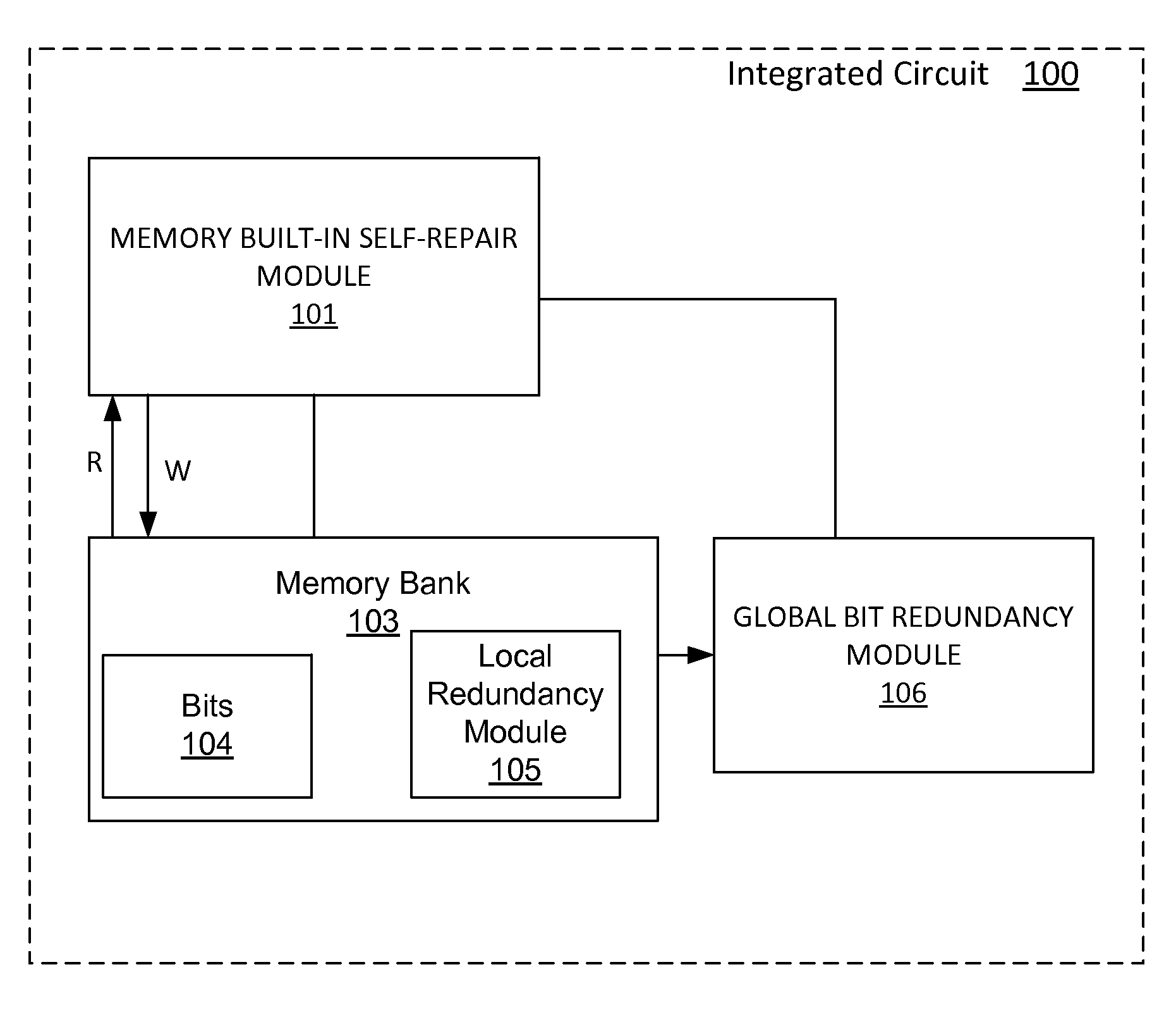
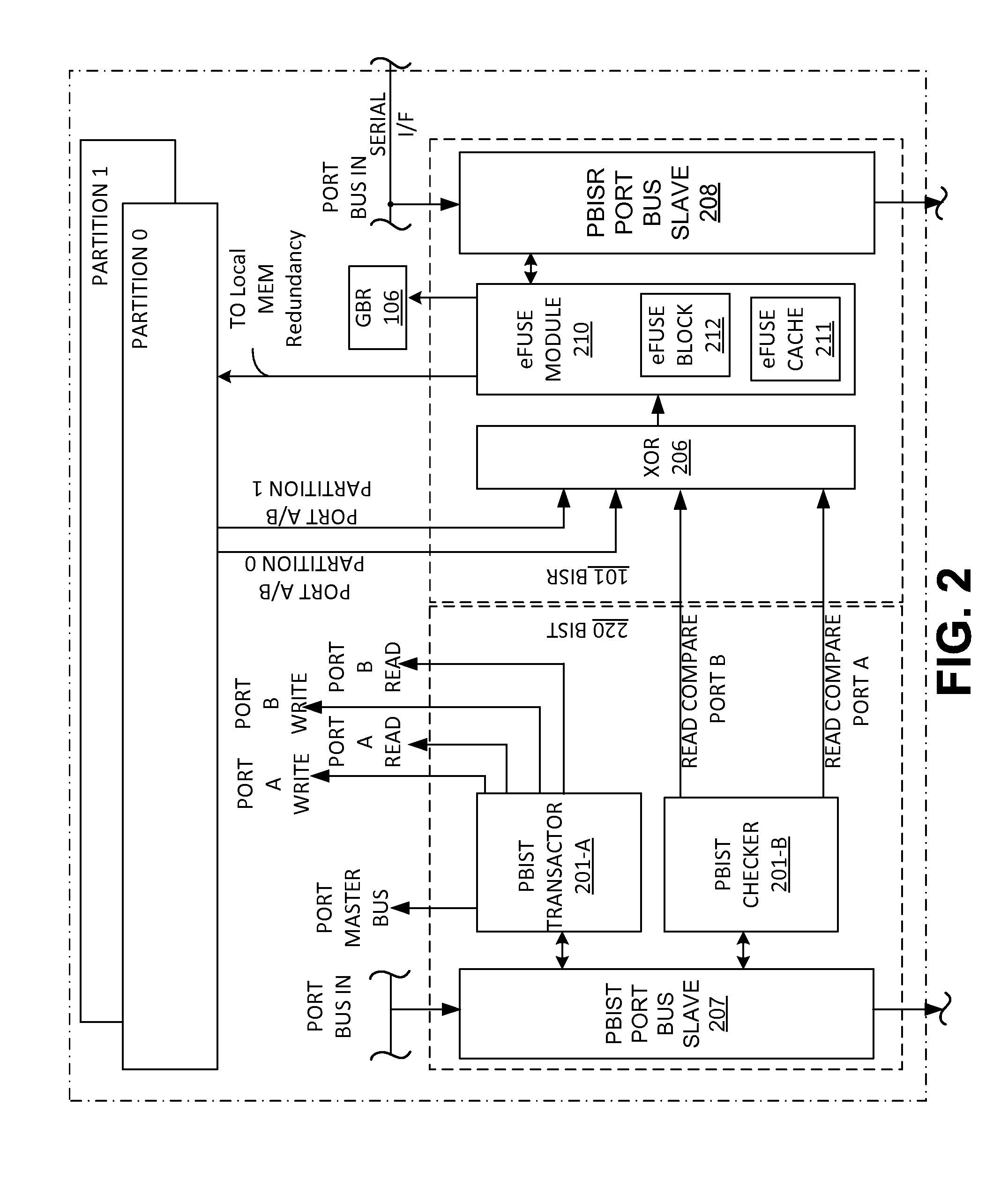
An integrated circuit chip comprising at least one programmable built-in self-repair (PBISR) for repairing memory is described. The PBISR comprises an interface that receives signals external to the integrated chip. The PBISR further includes a port slave module that programs MBISR registers, program and instruction memory. The PBISR further comprises a programmable transaction engine and a programmable checker. Further, the MBISR comprises an eFUSE cache that implements logic to denote defective elements.

Description

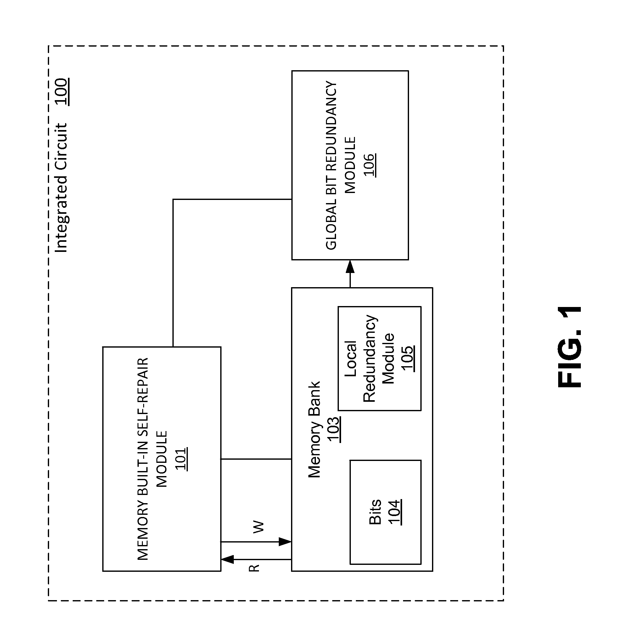
CROSS-REFERENCE TO RELATED U.S. APPLICATIONS[0001]This application claims priority to and benefit of co-pending U.S. Patent Application No. 61 / 702,732, filed on Sep. 18, 2012, entitled, “PROGRAMMABLE MEMORY BUILT IN SELF REPAIR CIRCUIT,” by Rajesh Chopra, having Attorney Docket No. MP-1240.PRO, and assigned to the assignee of the present application.BACKGROUND[0002]Testing memories in a chip has become increasingly critical as memories have increased in complexity and density. The shrinking of geometries has even grater effect upon memories due to their tight layout hence creating new failure modes. These failure modes can be detected by a high speed tester. High speed testers are expensive and they need dedicated access to the memories.DISCLOSURE OF THE INVENTION[0003]An integrated circuit chip comprising at least one memory built-in self-repair (MBISR) is described. The MBISR comprises an interface that receives signals external to the integrated chip. The MBISR further includes a...

Claims


Application Information

Patent Timeline
IPC IPC(8): G11C29/04
CPCG11C29/4401G11C2029/4402G11C29/04
Inventor CHOPRA, RAJESH
Owner MOSYS INC
Learn More