Directed self assembly of block copolymers to form vias aligned with interconnects

a technology of photoresists and copolymers, which is applied in the direction of electrical equipment, semiconductor devices, semiconductor/solid-state device details, etc., can solve the problems of lwr and/or cdu characteristics of photoresists generally needing to improve, and the critical dimensions of the via opening generally tend to scale faster than the resolution capability,

Inactive Publication Date: 2014-04-03
INTEL CORP
View PDF5 Cites 29 Cited by
  • Summary
  • Abstract
  • Description
  • Claims
  • Application Information

AI Technical Summary

Problems solved by technology

When patterning extremely small vias with extremely small pitches by such lithographic processes, several challenges present themselves, especially when the pitches are around 70 nanometers (nm) or less and / or when the critical dimensions of the via openings are around 35 nm or less.
One such challenge is that the overlay between the vias and the overlying interconnects, and the overlay between the vias and the underlying landing interconnects, generally need to be controlled to high tolerances on the order of a quarter of the via pitch.
Another such challenge is that the critical dimensions of the via openings generally tend to scale faster than the resolution capabilities of the lithographic scanners.
However, the shrink amount tends to be limited by the minimum via pitch, as well as by the ability of the shrink process to be sufficiently optical proximity correction (OPC) neutral, and to not significantly compromise line width roughness (LWR) and / or critical dimension uniformity (CDU).
Yet another such challenge is that the LWR and / or CDU characteristics of photoresists generally need to improve as the critical dimensions of the via openings decrease in order to maintain the same overall fraction of the critical dimension budget.
However, currently the LWR and / or CDU characteristics of most photoresists are not improving as rapidly as the critical dimensions of the via openings are decreasing.
A further such challenge is that the extremely small via pitches generally tend to be below the resolution capabilities of even extreme ultraviolet (EUV) lithographic scanners.
As a result, commonly two, three, or more different lithographic masks may be used, which tend to increase the costs.
At some point, if pitches continue to decrease, it may not be possible, even with multiple masks, to print via openings for these extremely small pitches using EUV scanners.

Method used


Image

  • Directed self assembly of block copolymers to form vias aligned with interconnects
  • Directed self assembly of block copolymers to form vias aligned with interconnects
  • Directed self assembly of block copolymers to form vias aligned with interconnects

Examples


Embodiment Construction

[0016]In the following description, numerous specific details, such as specific types of block copolymers, specific interconnect structures, specific orders of operations, specific materials, and the like, are set forth. However, it is understood that embodiments of the invention may be practiced without these specific details. In other instances, well-known structures and techniques have not been shown in detail in order not to obscure the understanding of this description.

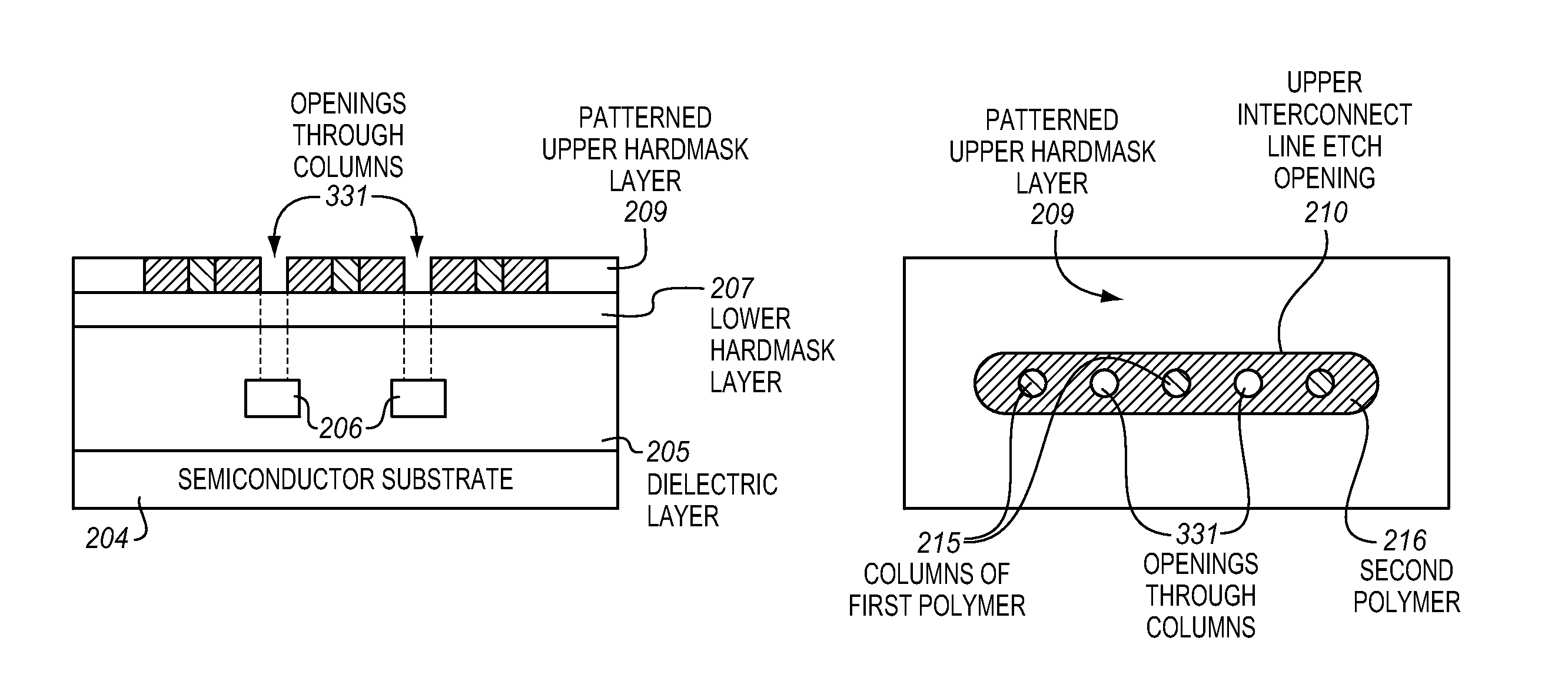
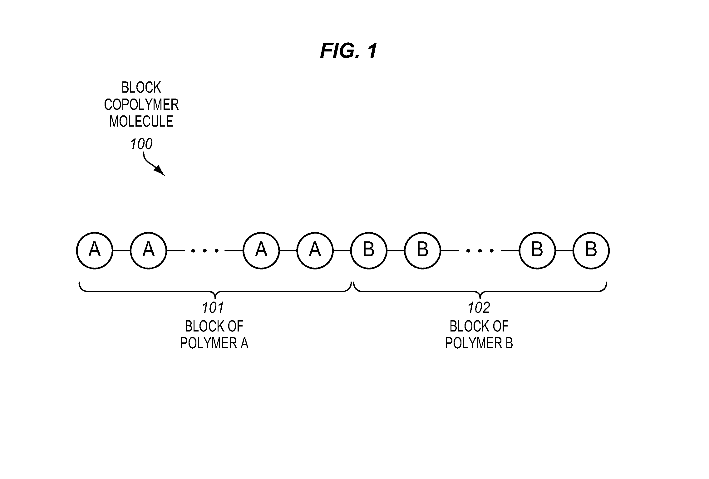
[0017]FIG. 1 illustrates a block copolymer molecule 100. The block copolymer molecule is a polymeric molecule formed of a chain of covalently bonded monomers. In a block copolymer, there are at least two different types of monomers, and these different types of monomers are primarily included within different blocks or contiguous sequences of monomers. The illustrated block copolymer molecule includes a block of polymer A 101 and a block of polymer B 102. The block of polymer A includes predominantly a chain of c...


PUM


Abstract

A method of an aspect includes forming an interconnect line etch opening in a hardmask layer. The hardmask layer is over a dielectric layer that has an interconnect line disposed therein. The interconnect line etch opening is formed aligned over the interconnect line. A block copolymer is introduced into the interconnect line etch opening. The block copolymer is assembled to form a plurality of assembled structures that are spaced along a length of the interconnect line etch opening. An assembled structure is directly aligned over the interconnect line that is disposed within the dielectric layer.

Description

BACKGROUND[0001]1. Field[0002]Embodiments relate to the field of integrated circuit manufacture. In particular, embodiments relate to forming openings for vias in integrated circuit manufacture.[0003]2. Background Information[0004]Integrated circuits commonly include electrically conductive microelectronic structures, which are known in the arts as vias, to electrically connect metal lines or other interconnects above the vias to metal lines or other interconnects below the vias. Vias are typically formed by a lithographic process. Representatively, a photoresist layer may be spin coated over a dielectric layer, the photoresist layer may be exposed to patterned actinic radiation through a patterned mask, and then the exposed layer may be developed in order to form an opening in the photoresist layer. Next an opening for the via may be etched in the dielectric layer by using the opening in the photoresist layer as an etch mask. This opening is referred to as a via opening. Finally, t...

Claims


Application Information

Patent Timeline
Patent Type & Authority Applications(United States)
IPC IPC(8): H01L21/768H01L23/522
CPCH01L21/0337H01L21/31144H01L21/76811H01L21/76816H01L23/5226H01L2924/0002H01L2924/00H01L21/76877
Inventor NYHUS, PAUL A.SIVAKUMAR, SWANINATHAN
Owner INTEL CORP
Why Eureka
Try Eureka