Method and system for producing component mounting board

a technology of component mounting and mounting plate, which is applied in the direction of final product manufacturing, sustainable manufacturing/processing, soldering apparatus, etc., can solve the problems of component mounting plate subject to repair work, electrical junction between the wiring board and the electronic component may be broken, etc., to achieve high joint strength between the wiring board and the electronic component, the effect of better understanding

Active Publication Date: 2014-06-12
PANASONIC INTELLECTUAL PROPERTY MANAGEMENT CO LTD
View PDF22 Cites 10 Cited by
  • Summary
  • Abstract
  • Description
  • Claims
  • Application Information

AI Technical Summary

Benefits of technology

[0012]According to the production method and system of the present invention, it is possible to produce a component mounting board in which the joining strength between the wiring board and the electronic component is high, and in repair work, poor junction is unlikely to occur between the wiring board and the electronic component.
[0013]While the novel features of the invention are set forth particularly in the appended claims, the invention, both as to organization and content, will be better understood and appreciated, along with other objects and features thereof, from the following detailed description taken in conjunction with the drawings.

Problems solved by technology

However, the solder fillet is insufficient for enhancing the joining strength, and when the component mounting board is exposed to external impact, the electrical junction between the wiring board and the electronic component may be broken.
When an improper mounting of the electronic component (e.g., poor junction) or a defect of the electronic component itself is detected in the produced component mounting board, the component mounting board is subjected to repair work.

Method used


Image

  • Method and system for producing component mounting board
  • Method and system for producing component mounting board
  • Method and system for producing component mounting board

Examples


Embodiment Construction

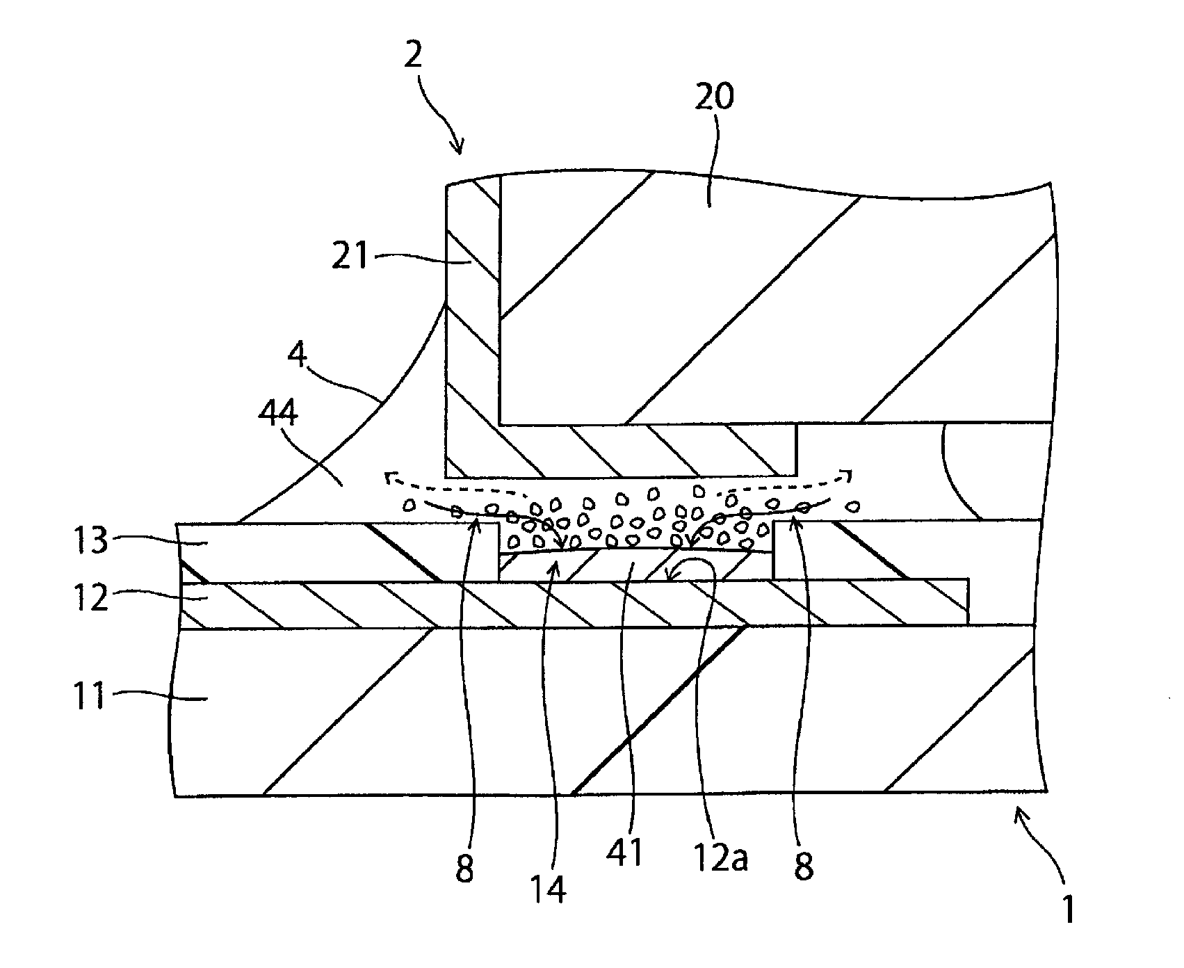
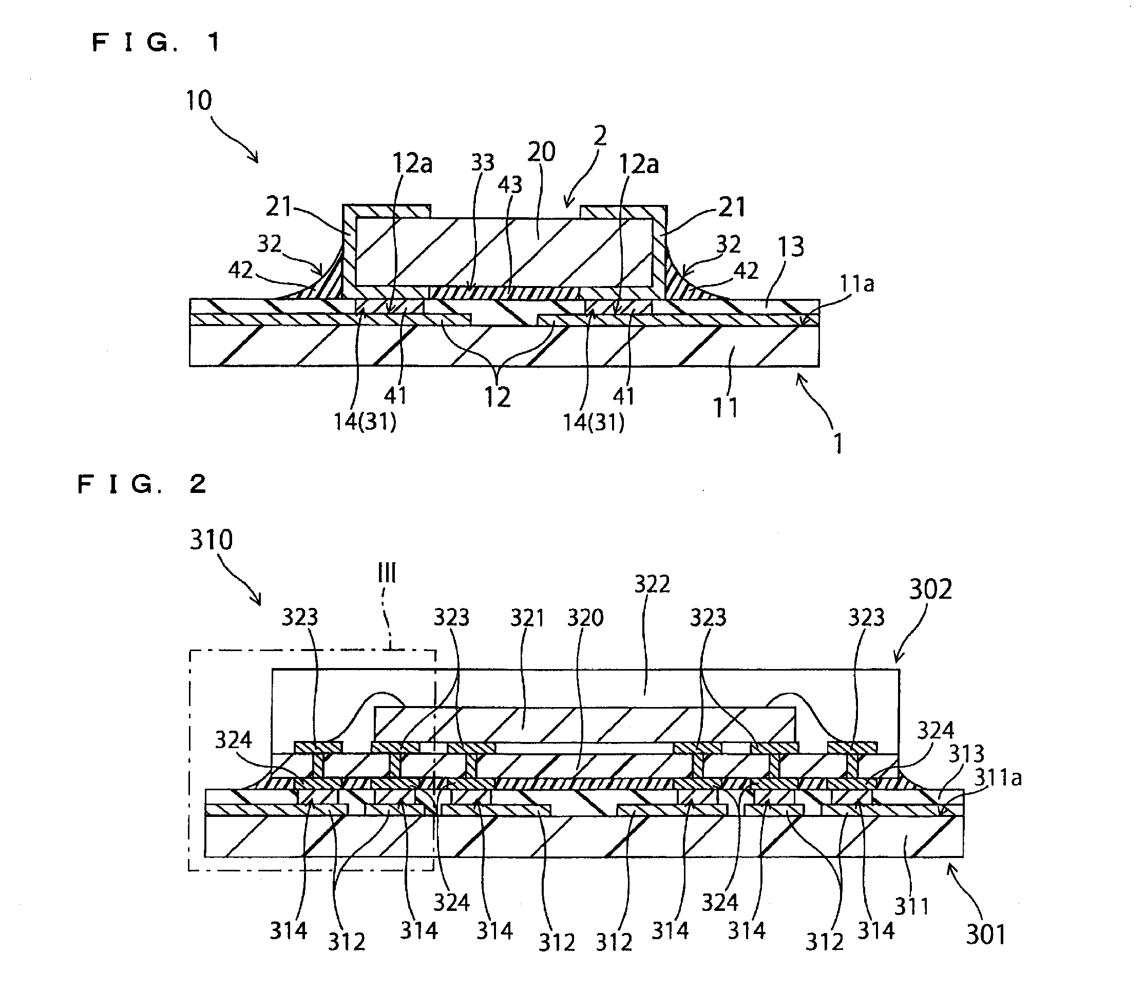
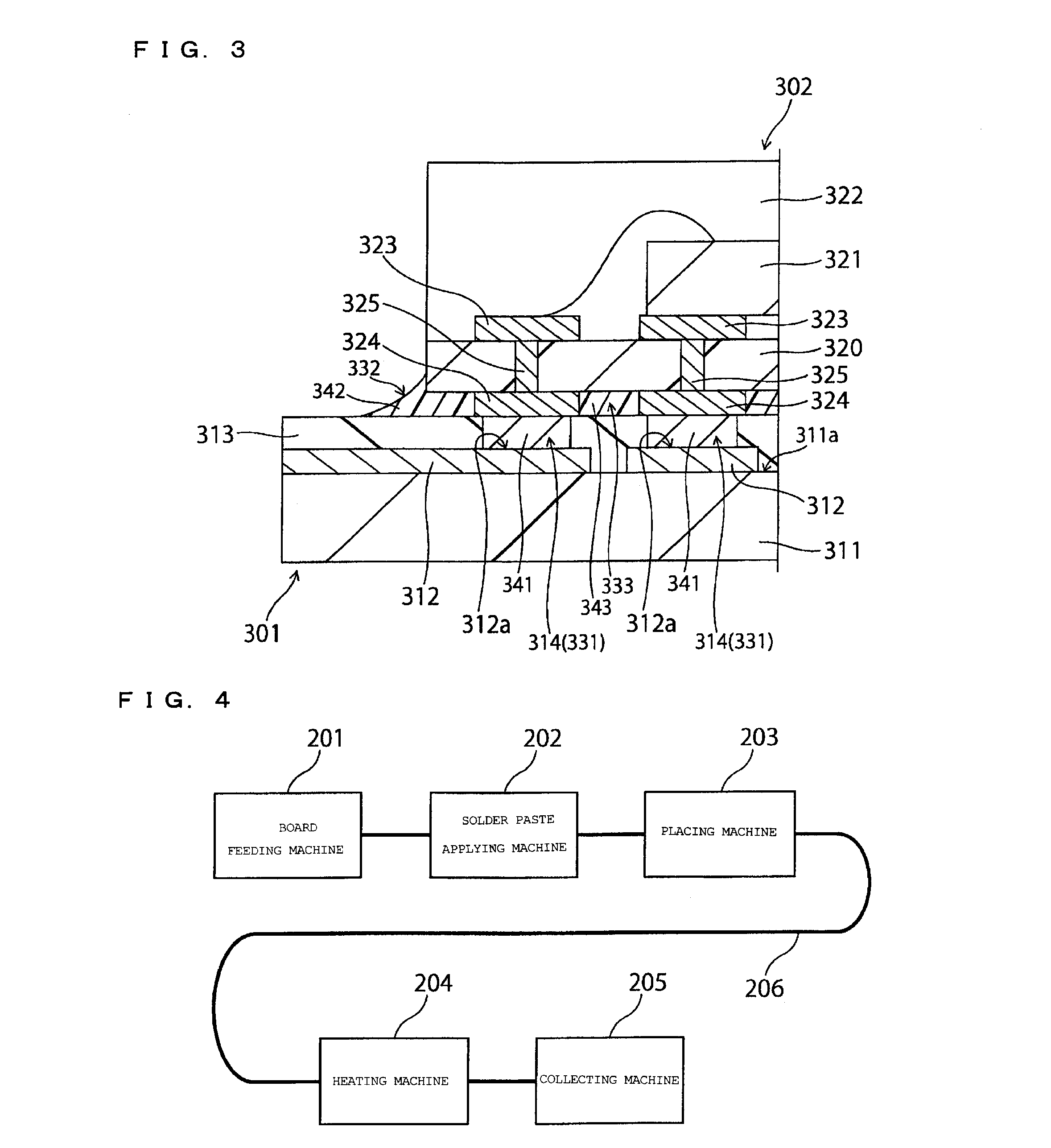
[0024]First, a description is given of a component mounting board produced by the production method and system according to the present invention.

[0025]The produced component mounting board includes a wiring board and an electronic component mounted on the wiring board. The wiring board includes an insulated board, a wiring layer formed on a surface of the insulated board, and a resist covering the wiring layer. The resist has an opening. The opening exposes from the resist, a joint face which is part of a surface of the wiring layer and to which a terminal of the electronic component is to be electrically joined, and the opening is entirely covered with the terminal.

[0026]A first space within the opening closed with the wiring layer and the electronic component is filled with solder, and the solder electrically joins the terminal and the joint face to each other. No thermosetting resin exists in the first space. Even if thermosetting resin exists in the first space, the amount ther...


PUM

PropertyMeasurementUnit
thicknessaaaaaaaaaa
thixotropicaaaaaaaaaa
total volumeaaaaaaaaaa

Abstract

A wiring board on which an electronic component is to be mounted includes a resist having an opening exposing a joint face which is part of the surface of a wiring layer and to which a terminal of the electronic component is to be joined. In the placing step, the electronic component is placed on the wiring board such that the terminal covers the opening entirely and contacts the solder paste applied onto the joint face. Next, the solder paste applied onto the joint face is heated to melt solder and soften thermosetting resin. This allows the solder to gather in a first space within the opening closed with the wiring layer and the electronic component, while allowing the thermosetting resin to gather in a second space formed between a top side of the resist and a lateral side of the electronic component.

Description

TECHNICAL FIELD[0001]The present invention relates to a method and a system for producing a component mounting board, and particularly relates to a technique for mounting an electronic component on a wiring board.BACKGROUND ART[0002]Low-melting-point solders have been conventionally used as a joining material for electrically joining an electronic component to a wiring board. Conventionally, in order to enhance the joining strength between the wiring board and the electronic component, the solder serving to join them together has been formed in a fillet form. The solder formed in a fillet form is called a solder fillet. However, the solder fillet is insufficient for enhancing the joining strength, and when the component mounting board is exposed to external impact, the electrical junction between the wiring board and the electronic component may be broken.[0003]Under these circumstances, in order to further enhance the joining strength, one proposal suggests the use of a solder past...

Claims


Application Information

Patent Timeline
Patent Type & Authority Applications(United States)
IPC IPC(8): H05K13/04
CPCH01L2224/48091H01L2224/48227H05K3/3442H05K3/3452H05K3/3463H05K2201/099H05K2201/10977H01L21/4867H01L2224/73257H01L2224/81192H01L2224/81815H01L2224/81862H01L2224/83886H01L2224/8159H01L2224/816H01L2224/81885H01L2224/0556H01L24/29H01L24/32H01L24/81H01L24/83H01L24/98H01L2224/0401H01L2224/05548H01L2224/06181H01L2224/16235H01L2224/2929H01L2224/293H01L2224/06187H01L2924/01322Y02P70/50H01L2924/00014H01L2924/0665H01L2924/014H01L2924/00012H01L2924/00H05K13/0465
Inventor MOTOMURA, KOJIKISHI, ARATAMARUO, HIROKISUZUKI, YASUHIROMUNAKATA, HIRONORI
Owner PANASONIC INTELLECTUAL PROPERTY MANAGEMENT CO LTD
Why Eureka
Try Eureka