Semiconductor device

a technology of semiconductor devices and semiconductors, applied in the direction of semiconductor devices, basic electric elements, electrical appliances, etc., can solve the problems of reducing the aperture ratio of a pixel, degrading the display quality of an image, and increasing power consumption, so as to improve the aperture ratio and low power consumption

Active Publication Date: 2014-06-26
SEMICON ENERGY LAB CO LTD
View PDF7 Cites 38 Cited by
  • Summary
  • Abstract
  • Description
  • Claims
  • Application Information

AI Technical Summary

Benefits of technology

[0022]According to one embodiment of the present invention, a semiconductor device including a capacitor whose charge capacity is inc

Problems solved by technology

As a result, the number of times of rewriting image data is increased, so that power consumption is increased.
However, when the area of a light-blocking conductive film is increas

Method used


Image

  • Semiconductor device
  • Semiconductor device
  • Semiconductor device

Examples


embodiment 1

[0084]In this embodiment, a semiconductor device of one embodiment of the present invention is described with reference to drawings. Note that in this embodiment, a semiconductor device of one embodiment of the present invention is described taking a liquid crystal display device as an example.

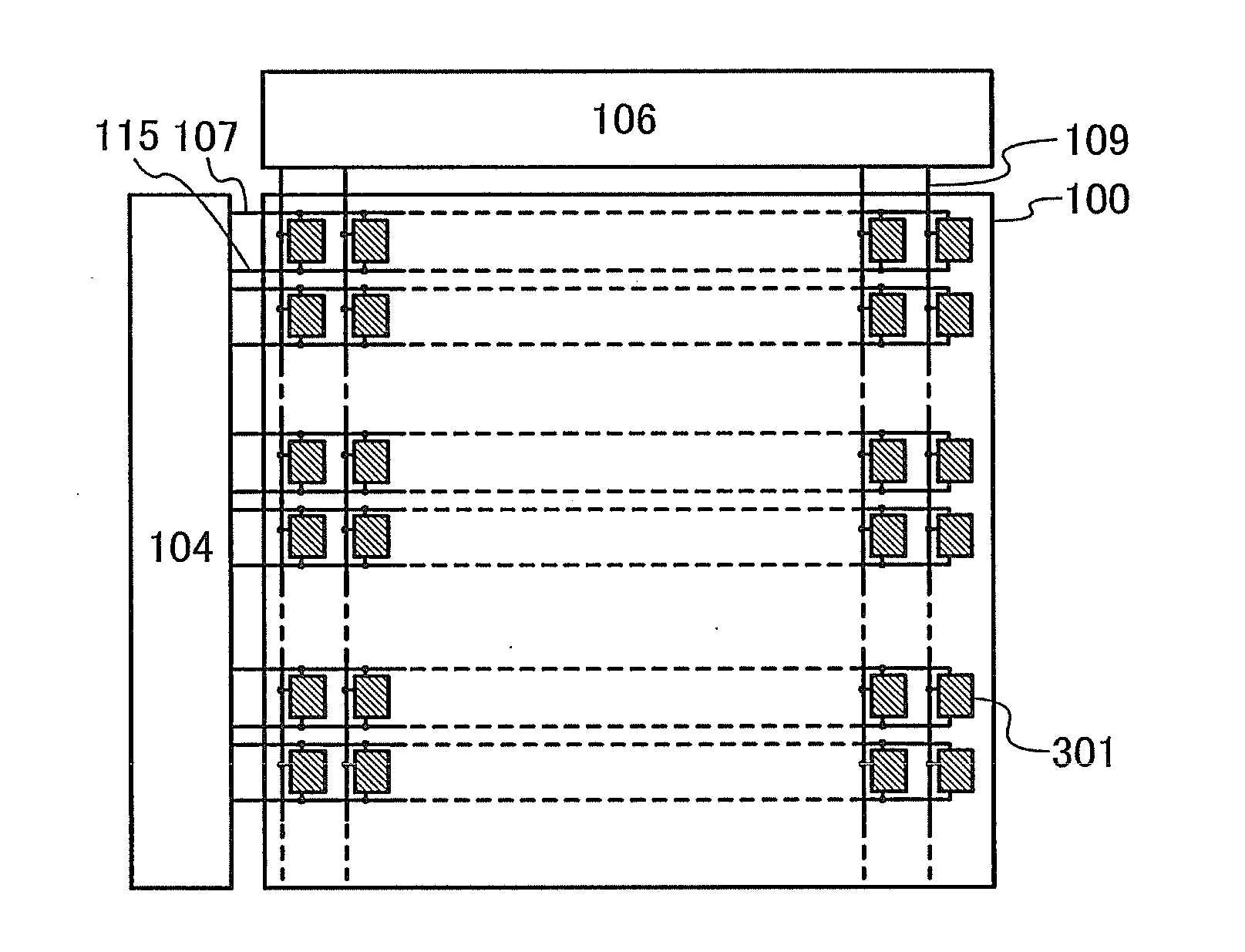
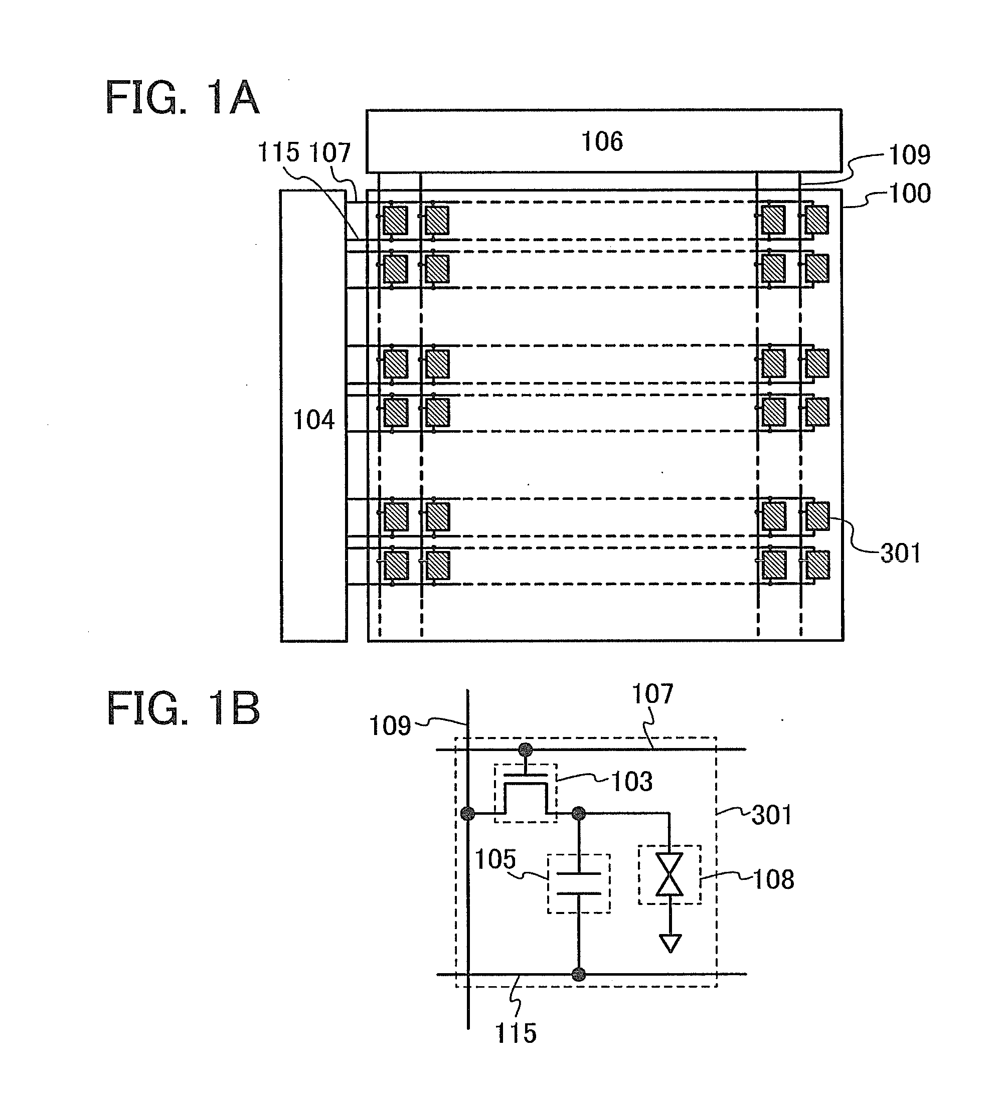
[0085]FIG. 1A illustrates an example of a semiconductor device. The semiconductor device in FIG. 1A includes a pixel portion 100, a scan line driver circuit 104, a signal line driver circuit 106, m scan lines 107 which are arranged in parallel or substantially in parallel and whose potentials are controlled by the scan line driver circuit 104, and n signal lines 109 which are arranged in parallel or substantially in parallel and whose potentials are controlled by the signal line driver circuit 106. Further, the pixel portion 100 includes a plurality of pixels 301 arranged in a matrix. Furthermore, capacitor lines 115 arranged in parallel or substantially in parallel are provided along the scan...

modification example 1

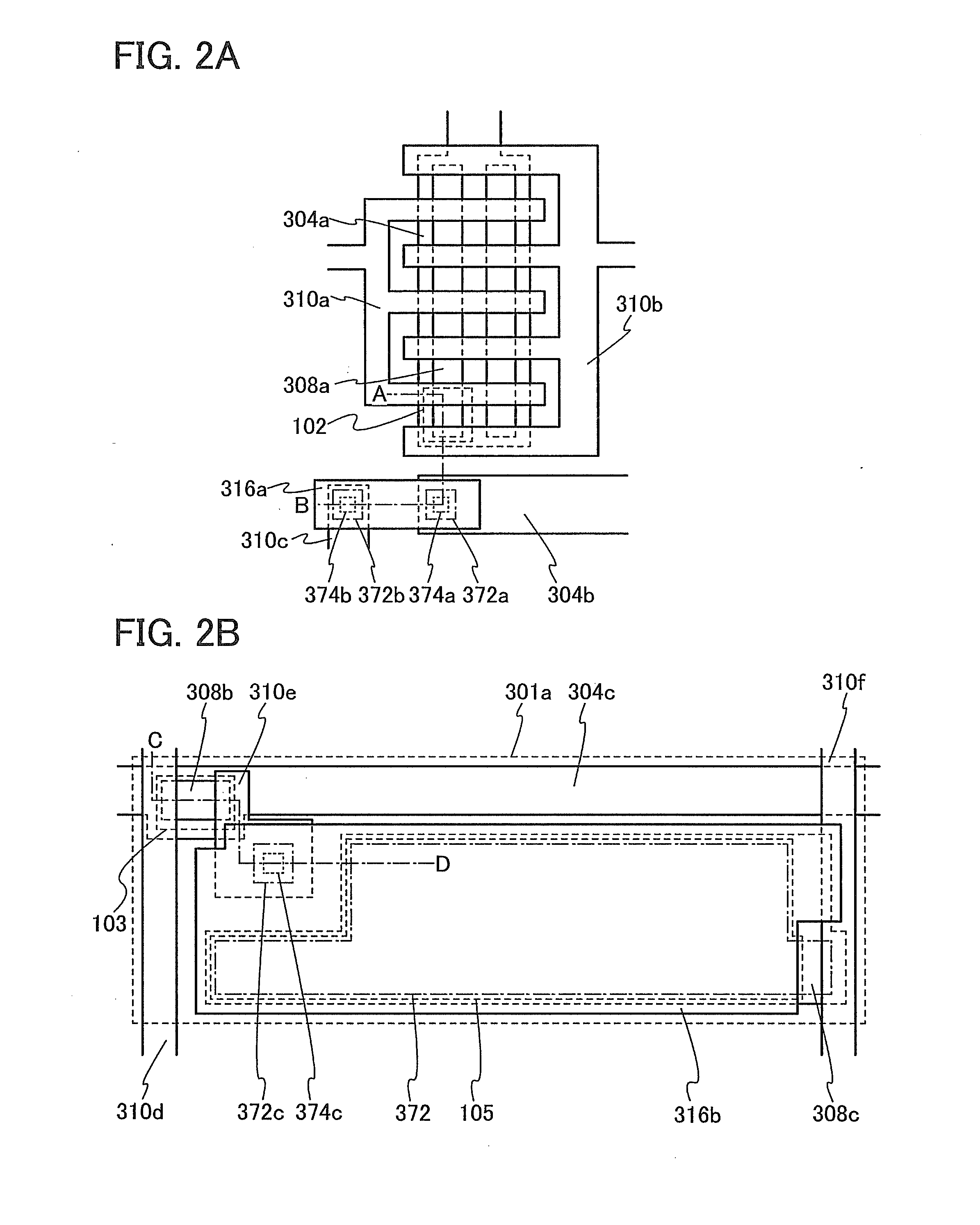
[0228]Here, a modification example of the pixel 301a of the semiconductor device described in Embodiment 1 is described with reference to FIGS. 3A to 3C and FIG. 9.

[0229]In FIG. 9, the conductive film 304c serving as a scan line is provided so as to extend perpendicularly or substantially perpendicularly to the signal line (in the horizontal direction in the drawing). The conductive film 310d serving as a signal line extends substantially perpendicularly to the scan line (in the vertical direction in the drawing). The conductive film 304d serving as a capacitor line is provided so as to extend in parallel with the scan line. The pixel 301b illustrated in FIG. 9 is different from the pixel 301a illustrated in FIG. 2B in that a side parallel to the conductive film 304c serving as a scan line is shorter than a side parallel to the conductive film 310d serving as a signal line, the conductive film 304d serving as a capacitor line extends in parallel to the scan line, and the conductive ...

modification example 2

[0234]Here, a modification example of the semiconductor device described in Embodiment 1 is described with reference to FIGS. 6A to 6C and FIG. 10.

[0235]A semiconductor device illustrated in FIG. 10 is different from the semiconductor device described in Embodiment 1 in that the insulating film 305, which is part of the gate insulating film, is in contact with the insulating film 314, which is part of the protective film, in a region between the conductive film 304b and the conductive film 310c. In other words, the insulating films 306 and 312 are not provided between the insulating film 305 and the insulating film 314 in the region between the conductive film 304b and the conductive film 310c.

[0236]Further, the insulating film 305, which is part of the gate insulating film, is in contact with the insulating film 314, which is part of the protective film, in a region between the conductive film 310e and the light-transmitting conductive film 308c. In other words, the insulating fil...


PUM


Abstract

A semiconductor device includes a transistor including an insulating film, an oxide semiconductor film, a gate electrode overlapping with the oxide semiconductor film, and a pair of electrodes in contact with the oxide semiconductor film; a capacitor including a first light-transmitting conductive film over the insulating film, a dielectric film over the first light-transmitting conductive film, and a second light-transmitting conductive film over the dielectric film; an oxide insulating film over the pair of electrodes of the transistor; and a nitride insulating film over the oxide insulating film. The dielectric film is the nitride insulating film, the oxide insulating film has a first opening over one of the pair of electrodes, the nitride insulating film has a second opening over the one of the pair of electrodes, and the second opening is on an inner side than the first opening.

Description

TECHNICAL FIELD[0001]The present invention relates to an object, a process (including a method and a manufacturing method), a machine, a manufacture, or a composition of matter. In particular, one embodiment of the present invention relates to a semiconductor device, a display device, a light-emitting device, a driving method thereof, a manufacturing method thereof, or the like. In particular, one embodiment of the present invention relates to a semiconductor device, a display device, a light-emitting device, or the like each including an oxide semiconductor.[0002]In this specification, a semiconductor device includes all of the devices that can function by utilizing electronic characteristics of a semiconductor in its category, and for example, an electrooptic device, a semiconductor circuit, and electronic equipment are all included in semiconductor devices.BACKGROUND ART[0003]In recent years, flat panel displays such as liquid crystal displays (LCDs) have been widespread. In each...

Claims


Application Information

Patent Timeline
IPC IPC(8): H01L27/12
CPCH01L27/1225H01L27/1248H01L27/1255H01L27/124G09G3/3266G02F1/1362G09G2330/021G09G2300/0426
Inventor YAMAZAKI, SHUNPEIMIYAKE, HIROYUKISHISHIDO, HIDEAKIKATAYAMA, MASAHIROOKAZAKI, KENICHI
Owner SEMICON ENERGY LAB CO LTD
Why Eureka
Try Eureka