Adaptive digital delay line for characterization of clock uncertainties

a digital delay line and clock uncertainty technology, applied in the field of integrated circuit devices, can solve the problems of significant changes in duty cycle, skew rate, other timing uncertainties in signaling, and the inability to meet the design requirement, and achieve the effect of reducing the number of integrated circuit devices and reducing the number of devices

Active Publication Date: 2014-07-03
ADVANCED MICRO DEVICES INC
View PDF5 Cites 20 Cited by
  • Summary
  • Abstract
  • Description
  • Claims
  • Application Information

AI Technical Summary

Problems solved by technology

Variations in a semiconductor fabrication process can lead to non-identical performance between resulting integrated circuit (IC) devices.
Typically, these variations are manifested in variations in the doping concentration, dimensions, and other parameters of the transistors of the IC devices, and can result in significant

Method used


Image

  • Adaptive digital delay line for characterization of clock uncertainties
  • Adaptive digital delay line for characterization of clock uncertainties
  • Adaptive digital delay line for characterization of clock uncertainties

Examples


Embodiment Construction

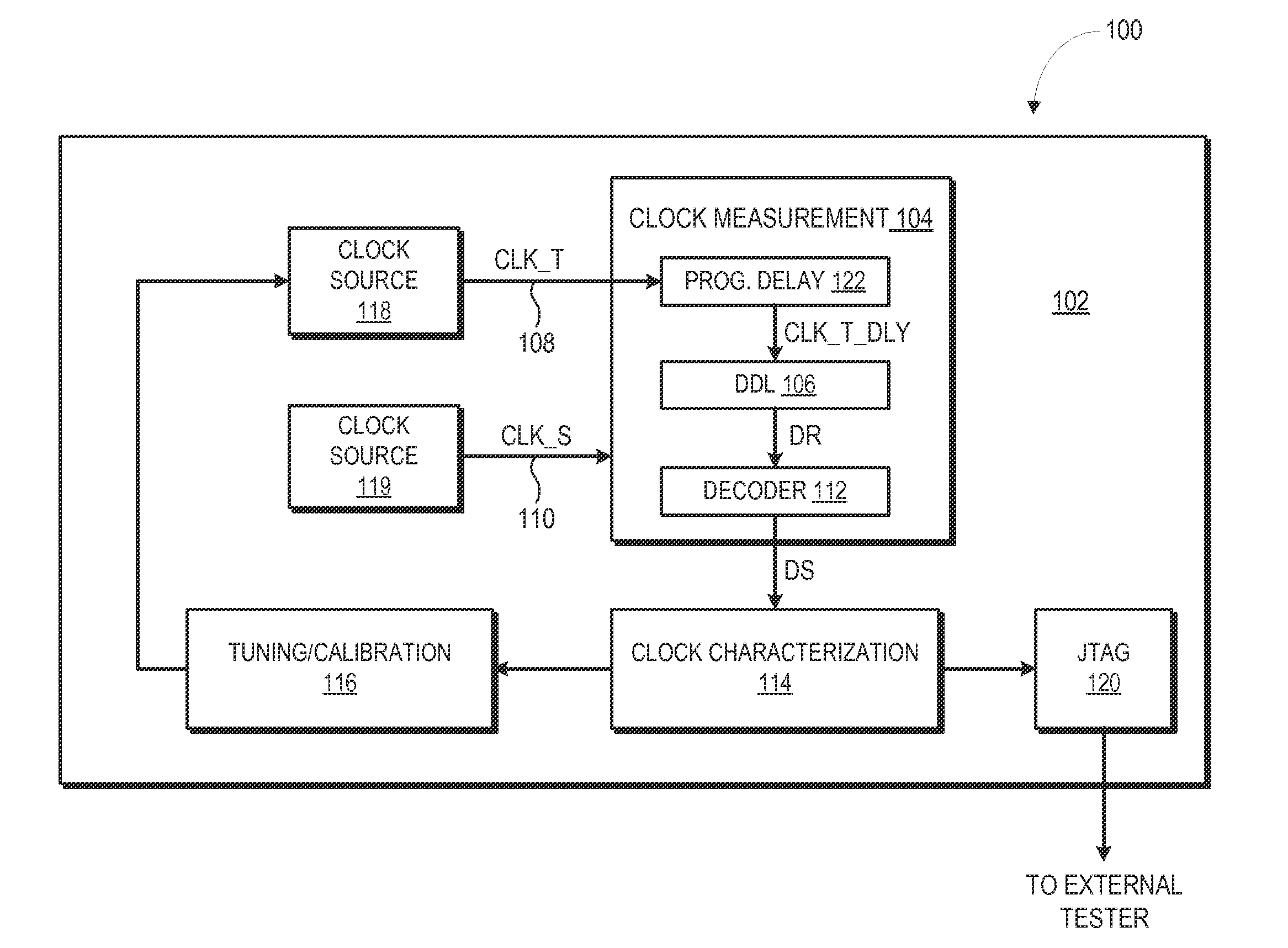
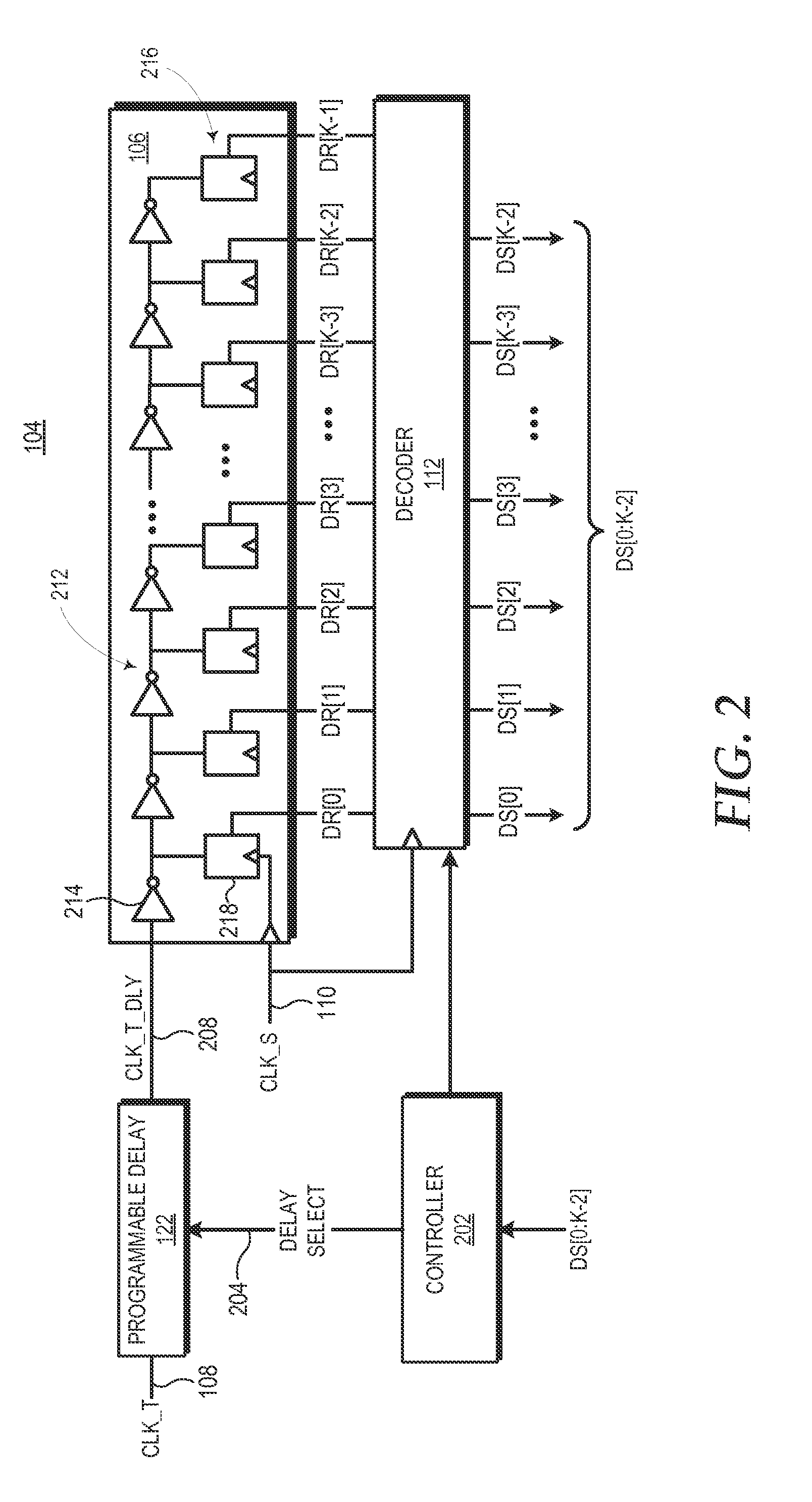
[0017]FIG. 1 illustrates an integrated circuit (IC) device 100 employing on-die clock measurement and characterization in accordance with some embodiments. The IC device 100 can comprise any of a variety of electrical components utilizing clock-synchronized circuitry, such as a central processing unit (CPU), graphics processing unit (GPU), digital signal processor (DSP) or other type of processor, an application specific integrated circuit (ASIC), and the like. A die 102 of the IC device 100 implements an on-die clock measurement circuit 104 that employs an adaptive digital delay line (DDL) 106 to obtain digital readings (denoted “DR”) for a test signal 108 (also denoted as “CLK_T”) at one or more process corners. The test signal 108 can comprise a clock signal or other signal to be characterized. The digital reading are measurements of a relationship between the test signal 108 and a sampling signal 110 (also denoted as “CLK_S”). The sampling signal 110 can include a clock signal f...


PUM


Abstract

An integrated circuit (IC) measures uncertainties in a first signal. The IC comprises a programmable delay circuit to introduce a programmable delay to the first signal to generate a first delayed signal. The IC further comprises a digital delay line (DDL) comprising a first delay chain of delay elements having input to receive the first delayed signal. The DDL further comprises a set of storage elements, each storage element having an input coupled to an output of a corresponding delay element of the first delay chain, and an output to provide a corresponding bit of a digital reading. The DDL additionally comprises a decoder to generate a digital signature from the digital reading and a controller to iteratively adjust the programmed delay of the programmable delay circuit to search for a failure in a resulting digital signature.

Description

BACKGROUND[0001]1. Field of the Disclosure[0002]The present disclosure relates generally to integrated circuit devices and more particularly to on-die signal measurement and characterization.[0003]2. Description of the Related Art[0004]Variations in a semiconductor fabrication process can lead to non-identical performance between resulting integrated circuit (IC) devices. Typically, these variations are manifested in variations in the doping concentration, dimensions, and other parameters of the transistors of the IC devices, and can result in significant changes to the duty cycle, skew rate, and other timing uncertainties in signaling conducted by the transistors. To accommodate these process variations, semiconductor device manufacturers may implement an on-die digital delay line (DDL) to obtain an on-die measurement of a timing characteristic of a signal.[0005]Typically, the DDL comprises a delay chain of inverters (or buffers) and a set of flip-flops to sample the output of each...

Claims


Application Information

Patent Timeline
IPC IPC(8): G01R29/00
CPCG01R31/31708G01R31/31726H03K5/14H03K5/133H03K5/1534
Inventor IYER, ARUN S.VALLUR, PRASHANTHPADIYAR, SHRADDHAGOVIL, AMIT
Owner ADVANCED MICRO DEVICES INC
Why Eureka
Try Eureka