
Solid-state image sensing device, image reading apparatus, and image forming apparatus

Active Publication Date: 2014-07-31
RICOH KK
View PDF5 Cites 42 Cited by
  • Summary
  • Abstract
  • Description
  • Claims
  • Application Information

AI Technical Summary

Benefits of technology

The patent text describes a new technology for improving the quality of images captured using a solid-state image sensing device. The technology includes a photoelectric conversion unit that converts light into electrical signals, a signal separation unit that removes unwanted signals caused by dark current, and a signal adding unit that adds the separated signals for each group of pixels. This results in a more accurate and reliable image. Additionally, the patent text describes an image reading apparatus that uses this new technology to process the captured images.

Problems solved by technology

However, in image sensors, dark current flows even when no light is incident.
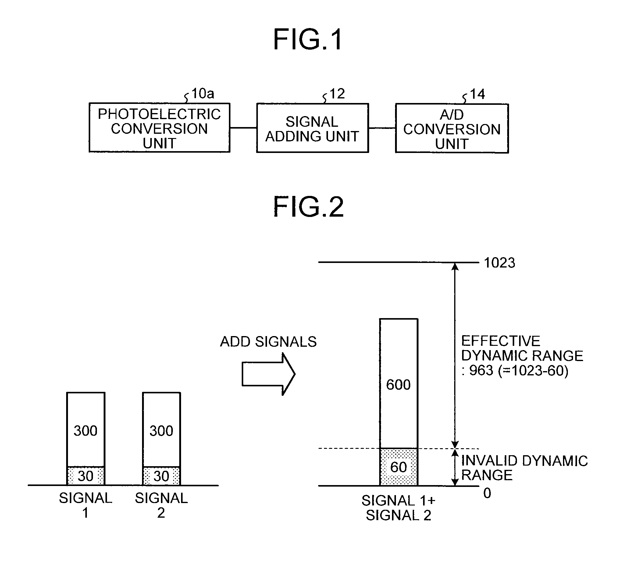
That is, when pixel signals including the offsets are added for resolution conversion, a dynamic range of image data after resolution conversion is disadvantageously narrowed.

Method used


Image

  • Solid-state image sensing device, image reading apparatus, and image forming apparatus
  • Solid-state image sensing device, image reading apparatus, and image forming apparatus
  • Solid-state image sensing device, image reading apparatus, and image forming apparatus

Examples


first embodiment

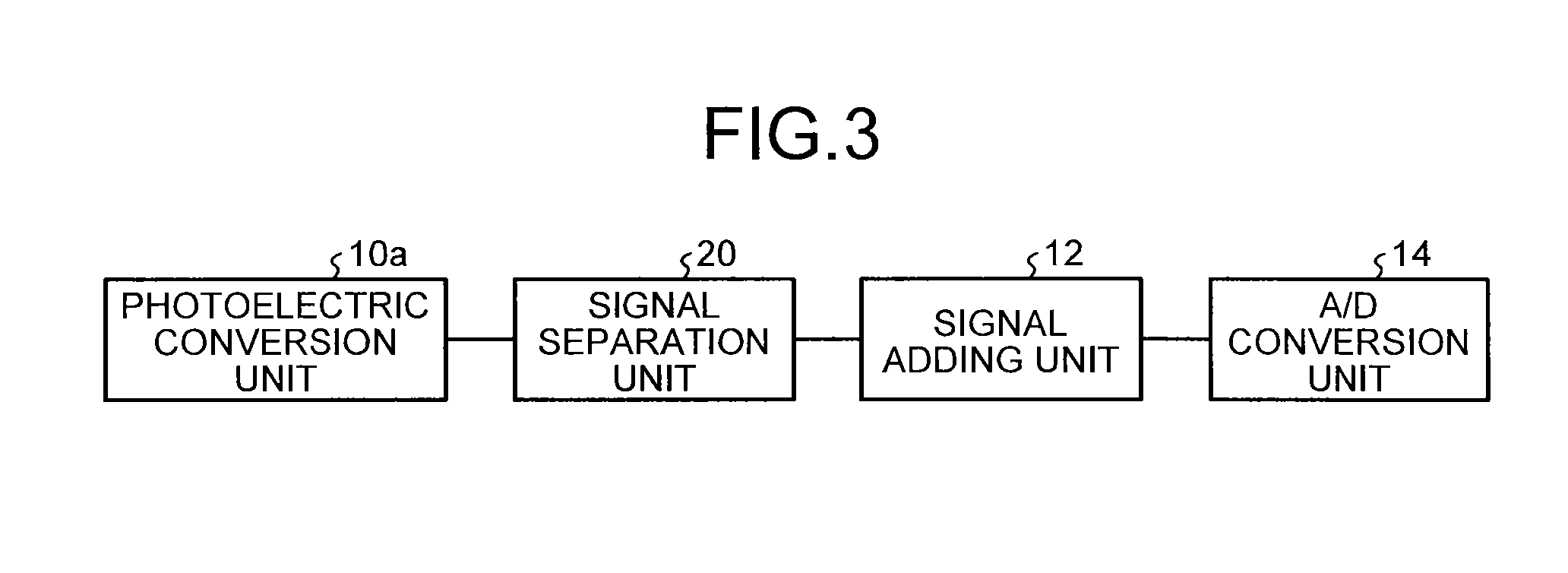
[0039]Next, a first embodiment of a solid-state image sensing device will be described in detail. FIG. 3 is a block diagram illustrating a schematic configuration of the solid-state image sensing device according to the first embodiment. The solid-state image sensing device according to the first embodiment is a CMOS linear image sensor, for example, and includes a photoelectric conversion unit 10a, a signal separation unit 20, a signal adding unit 12, and an A / D conversion unit 14. In the solid-state image sensing device illustrated in FIG. 3, component members substantially identical to those forming the solid-state image sensing device illustrated in FIG. 1 are designated by identical reference numerals.

[0040]The signal separation unit 20 separates (deletes) an offset signal, generated due to the dark current, from each of the electrical signals outputted by the photoelectric conversion unit 10a, and outputs, to the signal adding unit 12, image signals which are electrical signal...

second embodiment

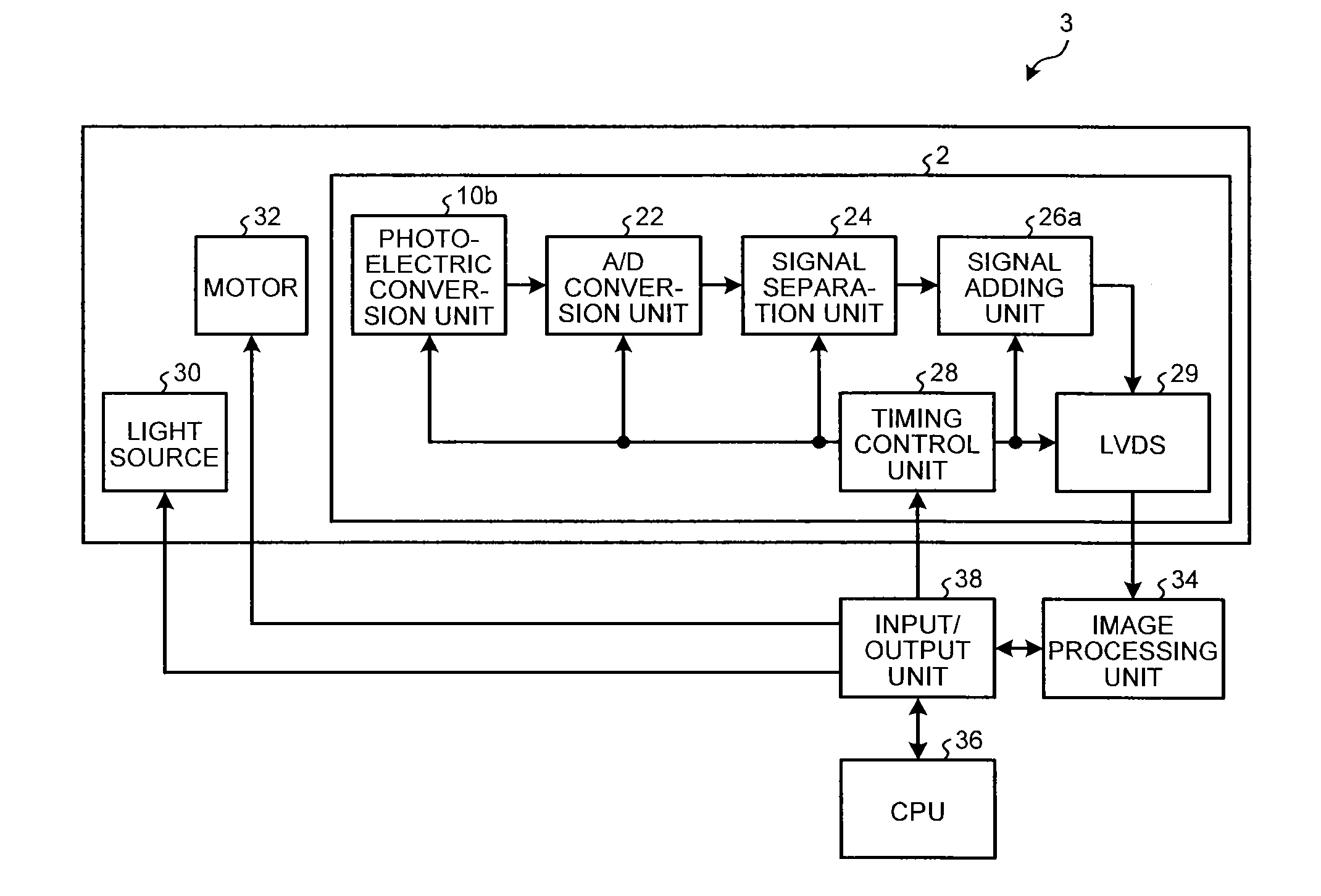
[0045]Next, a second embodiment of a solid-state image sensing device will be described in detail. FIG. 5 is a block diagram illustrating a schematic configuration of the solid-state image sensing device according to the second embodiment. The solid-state image sensing device according to the second embodiment is a CMOS linear image sensor, for example, and includes a photoelectric conversion unit 10b, an A / D conversion unit 22, a signal separation unit 24, and a signal adding unit 26a.

[0046]The photoelectric conversion unit 10b is formed by arraying a plurality of photoelectric conversion elements (not illustrated), such as photo diodes, to convert light into electrical signals for respective pixels and to output the converted electrical signals. The photoelectric conversion unit 10b outputs, to the A / D conversion unit 22, voltages corresponding to electric charge accumulated in accordance with light. The A / D conversion unit 22 converts the electrical signals, which have been outp...

first specific example

[0051]FIG. 6 is a block diagram illustrating a schematic configuration of a first specific example of the solid-state image sensing device according to the second embodiment. For example, as illustrated in FIG. 6, the first specific example of the solid-state image sensing device is a CMOS linear image sensor including a photoelectric conversion unit 10b, an A / D conversion unit 22, a signal separation unit 24, and a signal adding unit 26b. In the solid-state image sensing device illustrated in FIG. 6, component members substantially identical to those forming the solid-state image sensing device illustrated in FIG. 5 are designated by identical reference numerals.

[0052]The signal adding unit 26b adds image signals outputted by the signal separation unit 24 for each group of a plurality of consecutive pixels. Here, the signal adding unit 26b adds the image signals for each group of pixels the number of which corresponds to a ratio between resolutions before and after the resolution c...


PUM


Abstract

A solid-state image sensing device includes: a photoelectric conversion unit that converts light into electrical signals for respective pixels and outputs the electrical signals; a signal separation unit that separates an offset signal, which is generated due to dark current, from each of the electrical signals outputted by the photoelectric conversion unit and outputs image signals which are electrical signals converted from light for the respective pixels; and a signal adding unit that adds the image signals, which is outputted from the signal separation unit, for each group of a plurality of pixels.

Description

CROSS-REFERENCE TO RELATED APPLICATIONS[0001]The present application claims priority to and incorporates by reference the entire contents of Japanese Patent Application No. 2013-014518 filed in Japan on Jan. 29, 2013.BACKGROUND OF THE INVENTION[0002]1. Field of the Invention[0003]The present invention relates to a solid-state image sensing device, an image reading apparatus, and an image forming apparatus.[0004]2. Description of the Related Art[0005]A resolution conversion technique is conventionally known which increases an image reading rate and reduces the size of read image data by reading images at a resolution lower than the resolution at which the image reading apparatus can perform reading. By reading images at a lowered resolution, the amount of light emission from a reading light source can be kept down and thereby power saving can be achieved.[0006]In a case where the resolution in image reading is lowered to enhance the productivity in reading of a document, an image rea...

Claims


Application Information

Patent Timeline
IPC IPC(8): H04N1/193H04N5/369
CPCH04N1/0408H04N1/193H04N5/369H04N23/741H04N25/63H04N25/75
Inventor KONNO, YOSHIONAKAZAWA, MASAMOTO
Owner RICOH KK
Learn More