Surface-emitting laser and image forming apparatus using the same

a surface-emitting laser and image-forming technology, applied in semiconductor lasers, instruments, electrographic processes, etc., can solve the problems of delamination, short life span of devices, and complete destruction of surface-emitting lasers, so as to prevent delamination, improve reliability, and suppress voltage rise

Inactive Publication Date: 2014-08-14
CANON KK
View PDF4 Cites 2 Cited by
  • Summary
  • Abstract
  • Description
  • Claims
  • Application Information

AI Technical Summary

Benefits of technology

[0039]In view of the above-identified problems, an object of the present invention is to provide a surface-emitting laser that can prevent delamination at the interface of the selective oxidation layer and the spacer layer, while suppressing the voltage rise, and improve the reliability and also an image forming apparatus using the same.
[0041]Thus, the present invention can realize a surface-emitting laser that can prevent delamination at the interface of the selective oxidation layer and the spacer layer, while suppressing the voltage rise, and improve the reliability and also an image forming apparatus using the same.

Problems solved by technology

They degrade the interface quality and ultimately lead to a short life span of the device.
Such delamination is a problem specific to red surface-emitting lasers formed by using an AlGaInP-based material for the active region and an AlGaAs-based material for the DBR and having a current confinement structure produced by selective oxidation.
Such delamination can completely destruct the surface-emitting laser.
Thus, devices of the above-described type entail a poor yield in terms of good products and delamination can take place in operation to consequently destruct the device.
Particularly, destruction takes place in the inside and hence cannot be detected by an appearance inspection to make difficult to sort out good devices so that consequently the reliability of devices and hence entire systems such as image forming apparatus incorporating such devices will be degraded.

Method used


Image

  • Surface-emitting laser and image forming apparatus using the same
  • Surface-emitting laser and image forming apparatus using the same
  • Surface-emitting laser and image forming apparatus using the same

Examples


example 1

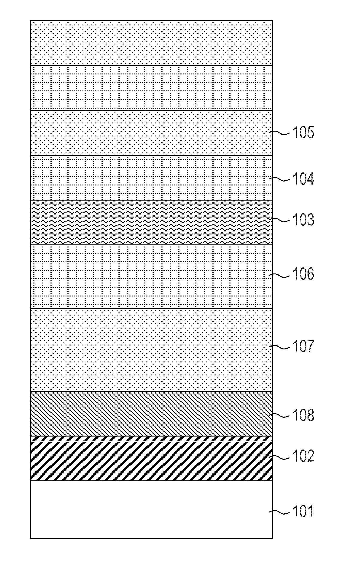
[0104]An exemplar configuration of the semiconductor laminated structure of the red surface-emitting laser of this example will be described below by referring to FIGS. 4 and 5.

[0105]The VCSEL structure of this example is formed by using the layers listed below.

[0106]It comprises an n-type GaAs substrate 401, an n-type DBR 402 formed by repetitively arranging n-type Al0.9Ga0.1As / Al0.5Ga0.5As, a spacer layer 403 formed by n-type Al0.35Ga0.15In0.5P, a barrier layer 404 formed by undoped Al0.25Ga0.25In0.5P, a quantum well active layer 405 formed by Ga0.56In0.44P / Al0.25Ga0.25In0.5P, a barrier layer 406 formed by undoped Al0.25Ga0.25In0.5P, a spacer layer 407 formed by p-type Al0.5In0.5P, a third p-type intermediate layer 408 formed by p-type Al0.35Ga0.15In0.5P, a second p-type intermediate layer 409 formed by p-type Al0.9Ga0.1As, a first p-type intermediate layer 410 formed by p-type Al0.5Ga0.5As, a selective oxidation layer 411 formed by p-type Al0.98Ga0.02As, a p-type Al0.5Ga0.5As lay...

example 2

[0154]Now, Example 2 of the present invention will be described below.

[0155]FIG. 7 is a schematic cross sectional view of red surface-emitting laser 700 according to the present invention, showing the layer arrangement thereof.

[0156]The VCSEL structure of this example is formed by using the layers listed below.

[0157]It comprises an n-type GaAs substrate 401, a DBR 402 formed by n-type AlAs / Al0.5Ga0.5As, a spacer layer 403 formed by n-type Al0.35Ga0.15In0.5P, a barrier layer 404 formed by undoped Al0.25Ga0.25In0.5P, a quantum well active layer 405 formed by Ga0.56In0.44P / Al0.25Ga0.25In0.5P, a barrier layer 406 formed by undoped Al0.25Ga0.25In0.5P, a spacer layer 407 formed by p-type Al0.5In0.5P, a third p-type intermediate layer 408 formed by p-type Al0.4Ga0.1In0.5P, a second p-type intermediate layer 409 formed by p-type Al0.95Ga0.05As, a first p-type intermediate layer 410 formed by p-type Al0.5Ga0.5As, a selective oxidation layer 411 formed by p-type Al0.98Ga0.02As, a DBR 412 form...

example 3

[0178]An image forming apparatus using a surface-emitting laser array light source formed by arranging a plurality of surface-emitting lasers having a configuration as illustrated above will be described below by referring to FIGS. 9A and 9B.

[0179]FIG. 9A is a schematic plan view of the image forming apparatus and FIG. 9B is a lateral view of the apparatus.

[0180]The laser beam output from a surface-emitting laser array light source 1114 that is designed to operate as recording light source is irradiated onto a rotating polygon mirror 1110 that is driven to rotate by a motor 1112 through a collimator lens 1120.

[0181]The laser beam irradiated to the rotating polygon mirror 1110 is reflected as a deflected beam whose emission angel continuously changes as the rotating polygon mirror 1110 rotates. The reflected laser beam is corrected for distortions and so on by an f-θ lens 1122 and irradiated to a photosensitive member 1100 by way of a reflector 1116.

[0182]The photosensitive member 11...


PUM


Abstract

A surface-emitting laser that can prevent delamination at the interface of a selective oxidation layer and a spacer layer, while suppressing any rise of voltage, to improve the reliability of operation.

Description

RELATED APPLICATIONS[0001]This application is a divisional of application Ser. No. 13 / 111,282, filed May 19, 2011. It claims benefit of that application under 35 U.S.C. §120, and claims benefit under 35 U.S.C. §119 of Japanese Patent Application No. 2010-121228, filed on May 27, 2010. The entire contents of each of the mentioned prior applications are incorporated herein by reference.BACKGROUND OF THE INVENTION[0002]1. Field of the Invention[0003]The present invention relates to a surface-emitting laser. More particularly, it relates to a surface-emitting laser having a current confinement structure obtained by oxidation and also to an image forming apparatus using the same.[0004]2. Description of the Related Art[0005]A vertical cavity surface-emitting laser (to be referred to as VCSEL hereinafter) emits a laser beam perpendicularly relative to the in-plane direction of a semiconductor substrate.[0006]A VCSEL is generally so configured as to have an active region sandwiched between ...

Claims


Application Information

Patent Timeline
Patent Type & Authority Applications(United States)
IPC IPC(8): H01S5/187G03G15/04
CPCG03G15/04H01S5/187B82Y20/00G03G15/326H01S5/18311H01S5/18358H01S5/34326H01S5/423G03G15/04072H01S5/3436H01S5/3022
Inventor INAO, YASUHISAIKUTA, MITSUHIROTAKEUCHI, TETSUYA
Owner CANON KK
Why Eureka
Try Eureka