Liquid crystal panel and electronic apparatus

a technology of electronic equipment and liquid crystal panels, applied in static indicating devices, instruments, non-linear optics, etc., can solve the problems of rapid disappearance of alignment disturbance and non-restored original state, and achieve the effect of reducing transmittance, increasing alignment stability during voltage application, and rapidly disappearing alignment disturban

Active Publication Date: 2014-08-21
JAPAN DISPLAY INC
View PDF5 Cites 7 Cited by
  • Summary
  • Abstract
  • Description
  • Claims
  • Application Information

AI Technical Summary

Benefits of technology

[0024]When five bend points are provided, fourth and fifth bend points may be provided around both sides of the third bend point. In this case, if the cross angle between the extension direction of a slit formed between the fourth and fifth bend points on both sides of the third bend point and the alignment direction of the liquid crystal layer is larger than 7°, the alignment stability around the center of the pixel region during voltage application pixel region can be increased.
[0026]With this pixel structure, the alignment stability in the slit end portion can be intensively increased.

Problems solved by technology

In the case of the liquid crystal panel being used at present, if the reverse twist phenomenon occurs, the original state is not restored after it has been left uncontrolled.
With this configuration, even though a reverse twist line grows beyond a bent region and reaches the center of the screen, alignment disturbance can rapidly disappear.

Method used


Image

  • Liquid crystal panel and electronic apparatus
  • Liquid crystal panel and electronic apparatus
  • Liquid crystal panel and electronic apparatus

Examples


example 1

(C) Pixel Structure Example 1

[0116]The pixel structure shown in FIG. 16 is identical to the pixel structure described with reference to FIG. 12 or 13 and supposes an FFS (Fringe Field Switching) type liquid crystal panel.

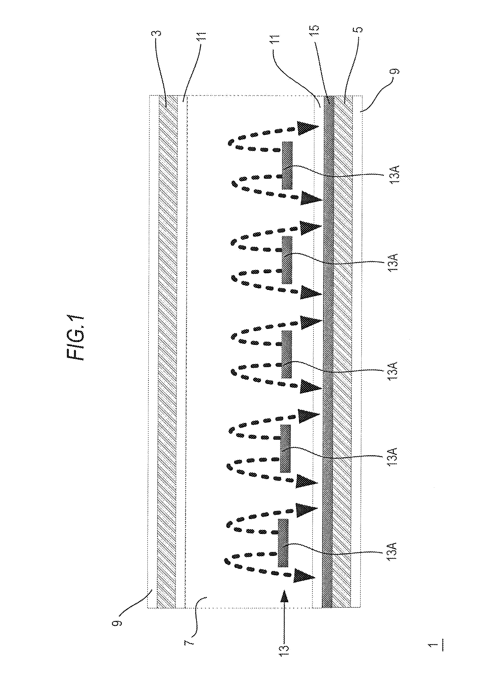
[0117]Thus, the sectional structure of the pixel region is as shown in FIG. 1. That is, the counter electrode 15 is disposed below the pixel electrode 13 so as to cover the entire pixel region.

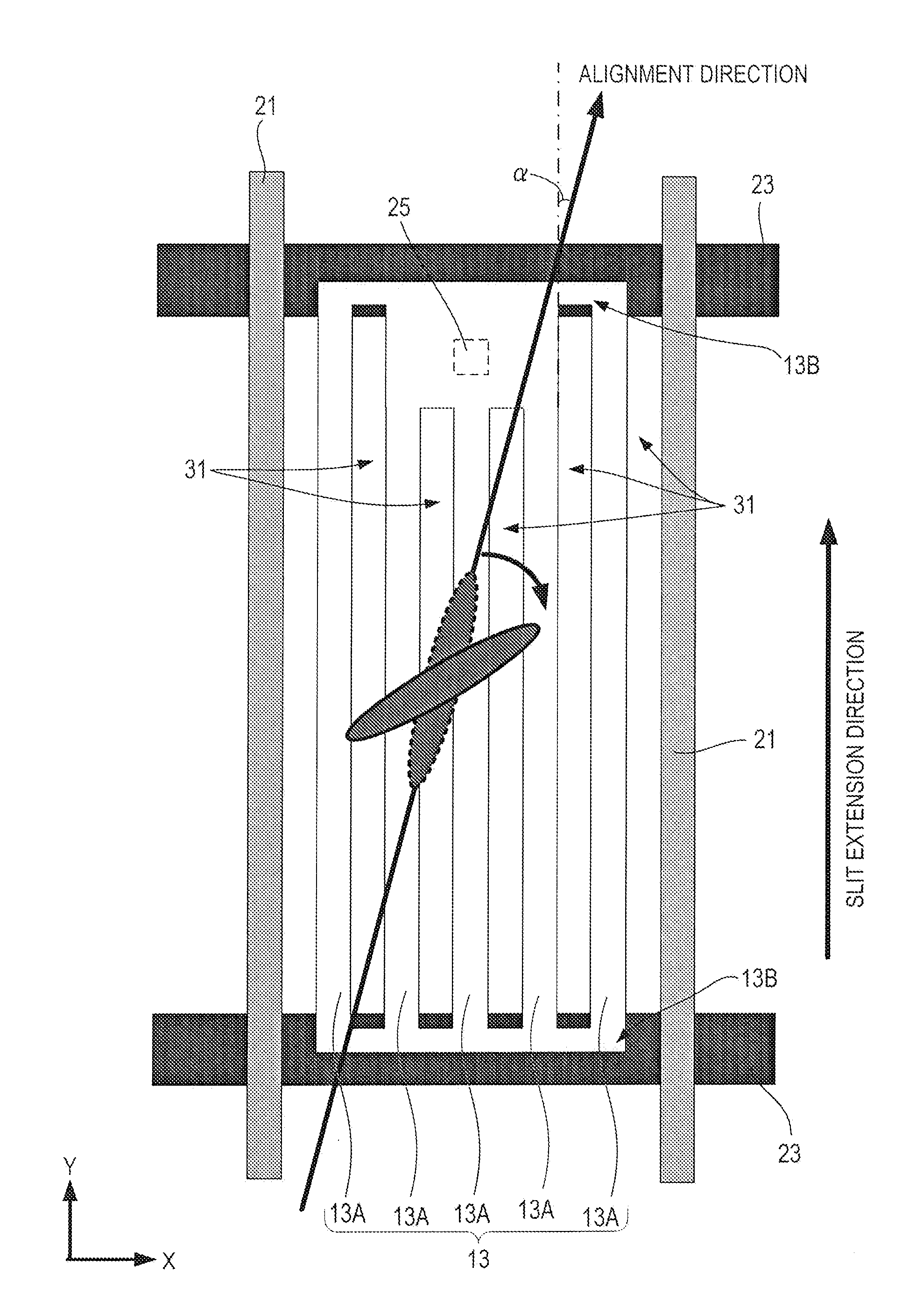
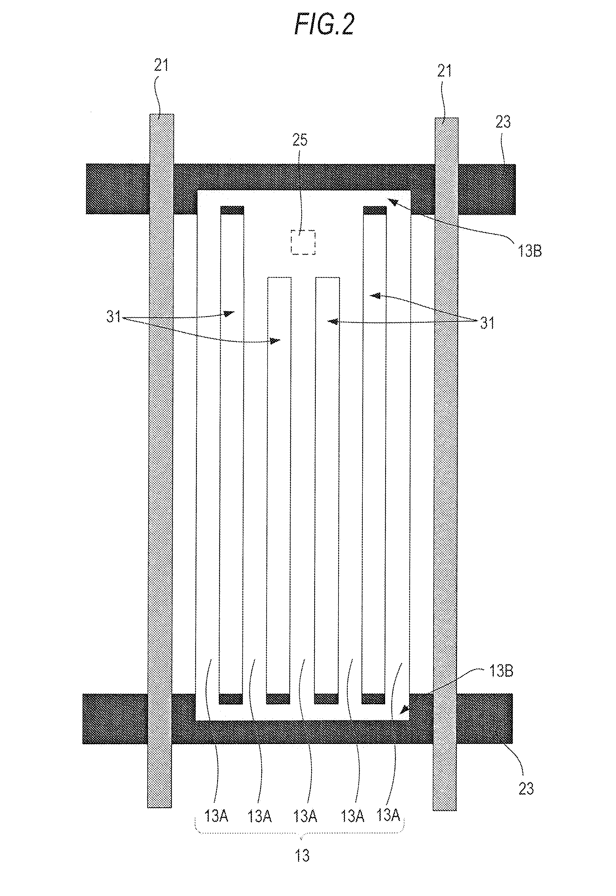
[0118]Like FIG. 12 or 13, the pixel structure shown in FIG. 16 is a pixel structure in which one bend point is provided. The bend point is provided around the contact 25. In FIG. 16, the area of the bent region is enlarged for ease of understanding of the extension direction of the slit 31 extending from the bend point toward the contact 25.

[0119]In FIG. 16, the extension direction of a slit 31 formed near the center of the pixel region from the bend point is parallel to the signal line 21. The extension direction of the slit 31 extending from the bend point toward the contact...

example 2

(D) Pixel Structure Example 2

[0125]FIG. 17 shows a second pixel structure example. This pixel structure also supposes an FFS (Fringe Field Switching) type liquid crystal panel.

[0126]In FIG. 17, the cross angle α2 between the extension direction of each slit 31 formed in the pixel region excluding the bent region and the alignment direction of the liquid crystal layer 7 is equal to or larger than 7°. The cross angle α1 between the extension direction of each slit 31 formed in the bent region and the alignment direction of the liquid crystal layer 7 is equal to or larger than the above-described cross angle α2.

[0127]In this pixel structure, the cross angle α1 between the extension direction of each slit 31 corresponding to the bent region and the alignment direction of the liquid crystal layer 7 can be set to be equal to or larger than 7°, so as in the pixel structure example 1, the alignment stability can be increased and disclination growth can be suppressed.

[0128]In this pixel stru...

example 3

(E) Pixel Structure Example 3

[0130]FIG. 18 shows a third pixel structure example. This pixel structure also supposes an FFS liquid crystal panel.

[0131]This pixel structure is also identical to the above-described two pixel structures, and corresponds to a pixel structure example with a single domain structure. This pixel structure example has a feature that two bend points (bent regions) are provided. Specifically, a second bend point is provided around the connection portion 13B on the side opposite to the contact 25.

[0132]This is to increase the alignment regulation force around both ends of the electrode branches 13A so as to shorten the time until a reverse twist line disappears. Of course, in this pixel structure, disclination which occurs at the end portions of the electrode branches 13A on the side opposite to the contact 25 can also be suppressed.

[0133]In the pixel structure example of FIG. 18, the positions of the bend points and the bend directions are set to be mirror-sym...


PUM

PropertyMeasurementUnit
angleaaaaaaaaaa
angleaaaaaaaaaa
angleaaaaaaaaaa

Abstract

A liquid crystal panel includes: first and second substrates arranged to be opposite each other at a predetermined gap; a liquid crystal layer filled between the first and second substrates; alignment films; a counter electrode pattern formed on the first substrate; and a pixel electrode pattern formed on the first substrate so as to have a plurality of electrode branches, the extension direction of which is bent at one bend point provided near an upper pixel portion from the center of a pixel region, and which are connected at the end portion of at least the upper pixel portion or lower pixel portion, wherein the extension direction of a slit formed near the upper pixel portion from the bend point from among slits formed in the pixel electrode pattern crosses the alignment direction of the liquid crystal layer at an angle of 7° or larger.

Description

CROSS REFERENCES TO RELATED APPLICATIONS[0001]The present application is a divisional application of U.S. patent application Ser. No. 12 / 640,906, filed Dec. 17, 2009, which application claims priority to Japanese Priority Patent Application JP 2008-324781 filed in the Japan Patent Office on Dec. 19, 2008, the entire contents of which is hereby incorporated by reference.BACKGROUND[0002]The present application relates to a transverse electric field driving liquid crystal panel which performs rotation control of the arrangement of liquid crystal molecules in parallel to a substrate surface by a transverse electric field generated between a pixel electrode and a counter electrode. The present application also relates to an electronic apparatus having the liquid crystal panel mounted therein.2. DESCRIPTION OF THE RELATED ART[0003]At present, liquid crystal panels have various panel structures including a vertical electric field display type in which an electric field is generated in the ...

Claims


Application Information

Patent Timeline
Patent Type & Authority Applications(United States)
IPC IPC(8): G02F1/1337
CPCG02F2001/133749G02F1/1337G02F1/134363G02F1/133707G02F1/136286G09G3/3607G02F1/134372G02F1/133749
Inventor SAKURAI, YOSHIHIROTANAKA, HIRONAOOKUNO, HARUMIKOITO, TAKEO
Owner JAPAN DISPLAY INC
Why Eureka
Try Eureka