Silane coupling material, substrate, and device

a technology of silicon coupling material and substrate, applied in the direction of organic chemistry, instruments, chemistry apparatus and processes, etc., can solve problems such as pixels occurrence of leakage curren

Pending Publication Date: 2021-01-07
SONY CORP
View PDF0 Cites 0 Cited by
  • Summary
  • Abstract
  • Description
  • Claims
  • Application Information

AI Technical Summary

Benefits of technology

[0045]In the present embodiment, the silane coupling material that includes hydrocarbon groups having numbers of carbon atoms different from each other in A and B is synthesized as the silane coupling material. This makes it possible to bind, onto one surface of the substrate, silyl groups that are portions of a molecular structure of the silane coupling material represented by the general formula (1) described above and include functional groups having different numbers of carbon atoms by one process. In addition, it is possible to react the silane coupling material according to the present embodiment in both liquid phase reaction and vapor phase reaction.
[0046]As described above, as the silane coupling material according to the present embodiment, the silane coupling material that is represented by the general formula (1) and includes hydrocarbon groups having numbers of carbon atoms different from each other in A and B is synthesized, which makes it possible to simply perform surface treatment of the substrate or the like by silane coupling reaction under moderate conditions.
[0047]FIG. 4 schematically illustrates a cross-sectional configuration of a liquid crystal display element (the liquid crystal display element 1) according to a second embodiment of the present disclosure. For example, the liquid crystal display element 1 is used as a liquid crystal light valve (for example, a light modulation element 141R) of a projection display apparatus (a projection display apparatus 3, see FIG. 6) such as a projector to be described later. The liquid crystal display element 1 corresponds to a specific example of a “device” of the present disclosure.
[0048]For example, the liquid crystal display element 1 has a configuration in which a pixel circuit substrate 11 and a counter substrate 21 are opposed to each other with a liquid crystal layer 30 interposed therebetween. Alignment films 12 and 22 (inorganic oxide films) are respectively provided on surfaces opposed to the liquid crystal layer 30 of the pixel circuit substrate 11 and the counter substrate 21. A stacking structure of the pixel circuit substrate 11 and the alignment film 12 and a stacking structure of the counter substrate 21 and the alignment film 22 each correspond to the substrate 10 according to the first embodiment described above. Accordingly, in the present embodiment, the liquid crystal display element 1 has a configuration in which the surface treatment section 10X and a surface treatment section 20X are respectively formed on surfaces opposed to the liquid crystal layer 30 of the alignment film 12 and the alignment film 22.
[0049]For example, a pixel circuit layer including a transistor is provided on side of a surface, of the pixel circuit substrate 11, opposed to the liquid crystal layer 30 of a light-transmissive substrate, and a pixel electrode is provided on the pixel circuit layer for each pixel, for example (neither the pixel circuit layer nor the pixel electrode is illustrated). The pixel electrode is electrically coupled to the transistor, and the alignment film 12 is provided on the pixel electrode. Although not illustrated, for example, a polarizing plate is joined to a surface, of a substrate included in the pixel circuit substrate 11, opposite to the surface opposed to the liquid crystal layer 30. It is to be noted that a peripheral circuit for driving pixels is formed on a periphery (a peripheral region (not illustrated)) of a pixel region of the pixel circuit substrate 11.
[0050]For example, although not illustrated, a counter electrode common to all pixels is provided on side of a surface, of the counter substrate 21, opposed to the liquid crystal layer 30 of the light-transmissive substrate. The alignment film 22 is provided on the counter electrode. Although not illustrated, for example, a polarizing plate is joined to a surface, of a substrate included in the counter substrate 21, opposite to the surface opposed to the liquid crystal layer 30.

Problems solved by technology

However, for example, a SiO2 deposited film is highly hygroscopic, which causes an issue of occurrence of a leakage current among pixels.

Method used


Image

  • Silane coupling material, substrate, and device
  • Silane coupling material, substrate, and device
  • Silane coupling material, substrate, and device

Examples


first embodiment (

1. First Embodiment (A silane coupling material including two silyl groups having numbers of carbon atoms different from each other)

[0024]1-1. Silane Coupling Material

[0025]1-2. Surface Treatment Method of Substrate

[0026]1-3. Workings and Effects

second embodiment (

2. Second Embodiment (An example of a liquid crystal display element in which a surface of an inorganic alignment film is subjected to surface treatment with a silane coupling material)

[0027]2-1. Configuration of Liquid Crystal Display Element

[0028]2-2. Method of Manufacturing Liquid Crystal Display Element

[0029]2-3. Workings and Effects

3. Modification Example (An example of an reflective liquid crystal display element)

4. Application Examples
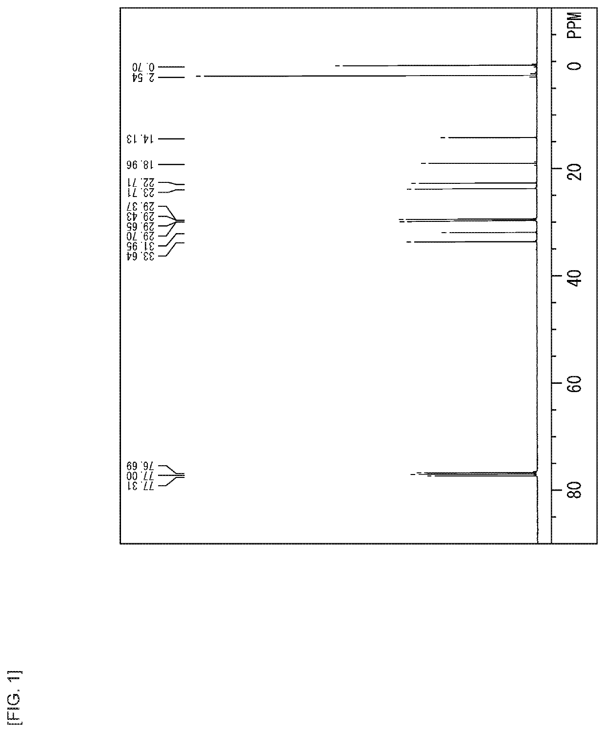
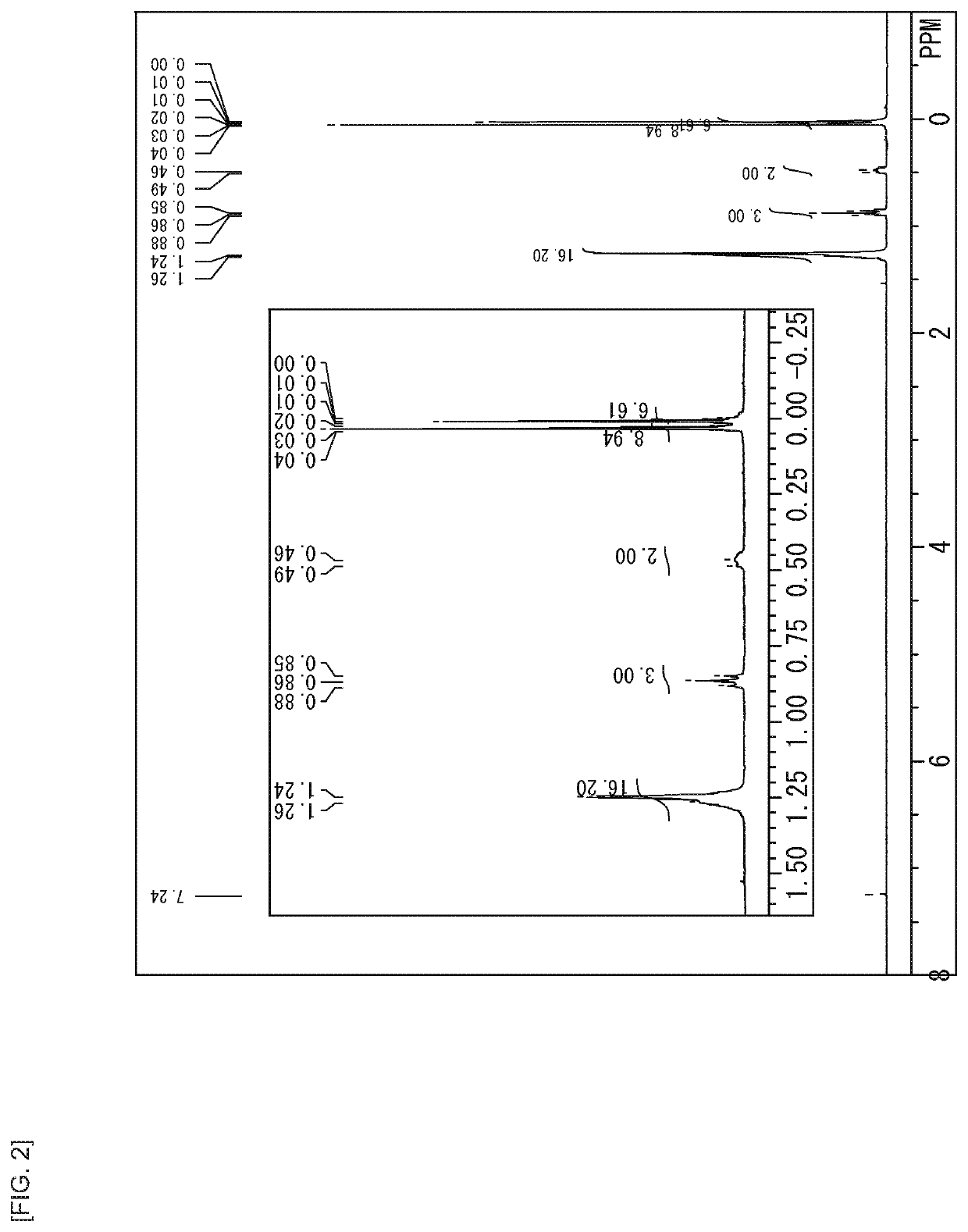
5. Examples

1. First Embodiment

(1-1. Silane Coupling Material)

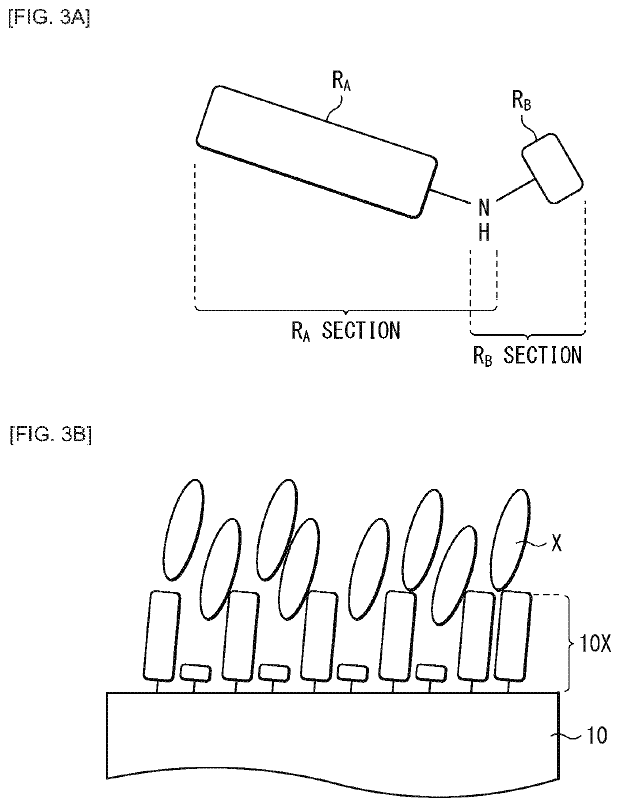
[0030]A silane coupling material according to a first embodiment of the present disclosure is represented by the following general formula (1). The silane coupling material makes it possible to add various kinds of functionality such as water repellency to a surface of a substrate 10 (see FIG. 3B), for example, by subjecting the substrate 10 to surface treatment. In addition, as described in detail later, for example, subjecting a surface of a substrate included in a liquid crystal dis...

second embodiment

2. Second Embodiment

[0047]FIG. 4 schematically illustrates a cross-sectional configuration of a liquid crystal display element (the liquid crystal display element 1) according to a second embodiment of the present disclosure. For example, the liquid crystal display element 1 is used as a liquid crystal light valve (for example, a light modulation element 141R) of a projection display apparatus (a projection display apparatus 3, see FIG. 6) such as a projector to be described later. The liquid crystal display element 1 corresponds to a specific example of a “device” of the present disclosure.

(2-1. Configuration of Liquid Crystal Display Element)

[0048]For example, the liquid crystal display element 1 has a configuration in which a pixel circuit substrate 11 and a counter substrate 21 are opposed to each other with a liquid crystal layer 30 interposed therebetween. Alignment films 12 and 22 (inorganic oxide films) are respectively provided on surfaces opposed to the liquid crystal laye...


PUM

PropertyMeasurementUnit
temperatureaaaaaaaaaa
pressureaaaaaaaaaa

Abstract

A silane coupling material according to an embodiment of the present disclosure is represented by the following general formula (1) and includes hydrocarbon groups having numbers of carbon atoms different from each other in A and B.

Description

TECHNICAL FIELD[0001]The present disclosure relates to a silane coupling material used, for example, for surface treatment of a substrate, and a substrate and a device subjected to surface treatment using the silane coupling material.BACKGROUND ART[0002]In recent years, a projection liquid crystal display apparatus (a projector) allowing for displaying on a brighter and large screen has been developed. In such a projector, extremely strong light enters a liquid crystal device as a light valve. Accordingly, the liquid crystal device typically uses an inorganic alignment film as an alignment film. For example, a deposited film including silicon oxide (SiO2) is used for the inorganic alignment film. However, for example, a SiO2 deposited film is highly hygroscopic, which causes an issue of occurrence of a leakage current among pixels.[0003]In contrast, for example, PTL 1 discloses a liquid crystal display element that suppresses chemical reaction with liquid crystal by subjecting a sur...

Claims


Application Information

Patent Timeline
Patent Type & Authority Applications(United States)
IPC IPC(8): C07F7/10G02F1/1337
CPCC07F7/10G02F1/133719G02F1/133734G02F2201/50G02F2201/501G02F2202/09G03B21/006
Inventor YAGI, YOSHITAKANAGASAWA, KOICHI
Owner SONY CORP
Why Eureka
Try Eureka