Display apparatus and electronic equipment

a technology of electronic equipment and display apparatus, applied in the direction of instruments, static indicating devices, etc., can solve the problems of vertical crosstalk, vertical crosstalk, vertical crosstalk, etc., and achieve the effect of reducing vertical crosstalk and compressed data lines

Active Publication Date: 2014-09-25
SEIKO EPSON CORP
View PDF3 Cites 8 Cited by
  • Summary
  • Abstract
  • Description
  • Claims
  • Application Information

AI Technical Summary

Benefits of technology

[0010]An advantage of some aspects of the invention is to provide a display apparatus and electronic equipment in which, even in the case of a display apparatus having a small pixel pitch, holding capacitors connected to data lines can be sufficiently ensured, so that the amplitude in the data lines can be compressed and vertical crosstalk can be reduced.

Problems solved by technology

Display apparatuses using light-emitting elements such as organic light-emitting diode (OLED) elements have a problem in which a change in signals in a data line adversely affects a pixel transistor, which leads to vertical crosstalk.
It was confirmed that the amplitude in the signal line at a drain contact portion of a pixel transistor actually affects the gate holding voltage at the drive transistor, which leads to vertical crosstalk.
However, it is not easy to form a holding capacitor having a predetermined area for each data line.
Accordingly, it is actually impossible to provide holding capacitors on the data lines within the range of the pixel pitch.
Writing of gradation voltages to the N first holding capacitors at different timings may cause crosstalk.
That is to say, a gradation voltage written to one of the N first holding capacitors at a certain timing adversely affects voltages of the data lines connected to the other first holding capacitors to which gradation voltages have been already written.
If the writing is limited to simultaneous writing, such a problem hardly occurs.

Method used


Image

  • Display apparatus and electronic equipment
  • Display apparatus and electronic equipment
  • Display apparatus and electronic equipment

Examples


Embodiment Construction

[0059]The following describes in detail a preferred embodiment of the invention. The embodiment set forth herein is not intended to unduly limit the scope of the invention defined in the claims, and not all of the structural features described in the embodiment are essential to the solution of the invention.

[0060]1. Display Apparatus (Electro-Optical Apparatus)

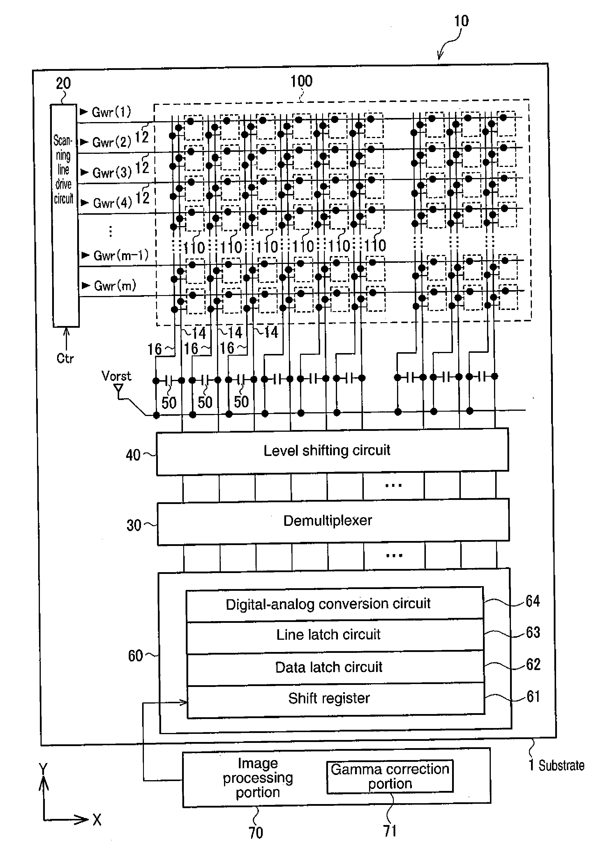
[0061]FIG. 1 shows a display apparatus (electro-optical apparatus) 10 of this embodiment. The display apparatus 10 is configured such that a scanning line drive circuit 20, a demultiplexer 30, a level shifting circuit 40, a data line drive circuit 60, and a display portion 100 are formed on a semiconductor substrate such as a silicon substrate 1.

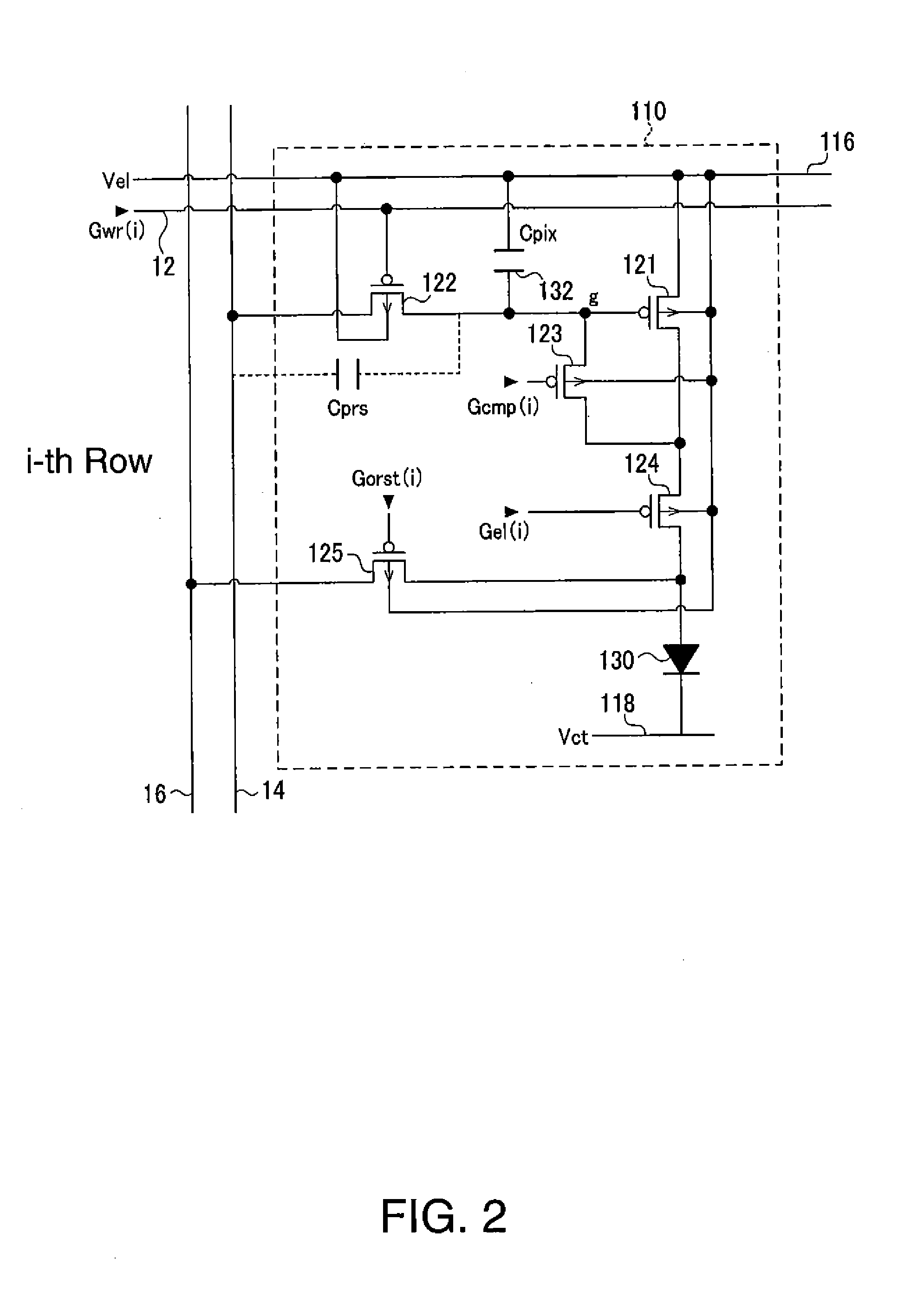
[0062]In the display portion 100, a plurality of scanning lines 12 are arranged in a row direction (horizontal direction), and a plurality of data lines 14 are arranged in a column direction (vertical direction) Y. A plurality of pixel circuits 110 each connected to one of the scanning...


PUM


Abstract

A plurality of pixel circuits provided in a display apparatus respectively include light-emitting elements OLED, first transistors that supply driving currents to the light-emitting elements, second transistors that turn on and off connection between data lines and gates of the first transistors, and third transistors. The display apparatus has first holding capacitors that are respectively inserted and connected midway on the plurality of data lines and shift levels of driving voltages of the first transistors, and holding capacitors that respectively hold potentials of the plurality of data lines. N first holding capacitors are arranged in a column direction Y, each of the first holding capacitors having an electrode width that is smaller than a width of N pixel circuits arranged adjacent to each other in a row direction X, and that is equal to or larger than a width of one pixel circuit.

Description

CROSS-REFERENCE TO RELATED APPLICATIONS[0001]This application claims priority to Japanese Patent Application No. 2013-060194 filed on Mar. 22, 2013. The entire disclosure of Japanese Patent Application No. 2013-060194 is hereby incorporated herein by reference.BACKGROUND[0002]1. Technical Field[0003]The present invention relates to a display apparatus, electronic equipment, and the like.[0004]2. Related Art[0005]Display apparatuses using light-emitting elements such as organic light-emitting diode (OLED) elements have a problem in which a change in signals in a data line adversely affects a pixel transistor, which leads to vertical crosstalk. In the related art, a shield line is provided between a data line and a pixel transistor inside a pixel (JP-A-2012-189828).[0006]It was confirmed that the amplitude in the signal line at a drain contact portion of a pixel transistor actually affects the gate holding voltage at the drive transistor, which leads to vertical crosstalk.[0007]In ord...

Claims


Application Information

Patent Timeline
Patent Type & Authority Applications(United States)
IPC IPC(8): G09G3/32
CPCG09G3/3208G09G2300/0861G09G2310/0248G09G2310/0289G09G2310/0297G09G2320/0209G09G3/2092
Inventor TAMURA, TSUYOSHINOMURA, TAKESHI
Owner SEIKO EPSON CORP
Why Eureka
Try Eureka