
Display device and method for driving same

a display device and display method technology, applied in the field of display devices, can solve the problems of increasing the load capacitance reducing the rate of change in the voltage of the source signal wire, and increasing the difficulty of writing the voltage of the desired picture signal in the pixel circuit, so as to achieve the effect of reducing vertical crosstalk and reducing the write period

Active Publication Date: 2014-05-29
JOLED INC
View PDF15 Cites 18 Cited by
  • Summary
  • Abstract
  • Description
  • Claims
  • Application Information

AI Technical Summary

Benefits of technology

The present invention is about a display device and a way to drive it that can accurately write pictures and reduce vertical crosstalk. This is even when the number of pixel rows and columns increases due to higher resolution screens and shorter write periods. With this invention, the device can accurately write pictures while minimizing interference between pixels, even at high resolution and faster writing speeds.

Problems solved by technology

In an active matrix display device using a liquid crystal element, an organic EL element, or the like, there is an increase in the load capacitance of the source signal wire 118 due to an increase in screen size or an increase in the number of vertical lines, and it is becoming increasingly difficult to write the voltage of a desired picture signal in a pixel circuit in a predetermined period (one horizontal scanning period).
In the case where the number of pixel rows has increased due to the increase in resolution of a display screen, the rate of change in the voltage of the source signal wire decreases, and it becomes further difficult to write a picture signal accurately.
In the case where the number of pixel columns has increased due to an increase in resolution of the display screen, the arrangement pitch of the source signal wire and the pixel circuit narrows, and therefore a leak current occurs.

Method used


Image

  • Display device and method for driving same
  • Display device and method for driving same
  • Display device and method for driving same

Examples


first embodiment

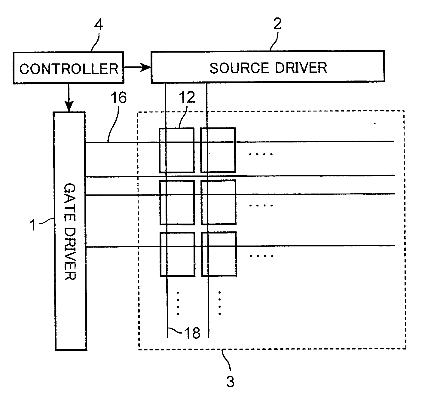
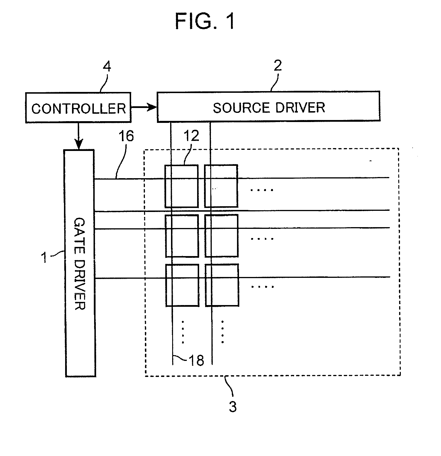
[0053]FIG. 1 is a block diagram showing the configuration of an active matrix display device in the present invention. In FIG. 1, a transistor 20 described later is omitted in the drawing in order to simplify the illustration.

[0054]The active matrix display device shown in FIG. 1 is an organic electro-luminescence (EL) display device and includes a gate driver 1, a source driver 2, an organic electro-luminescence (EL) panel 3, a controller 4, a plurality of gate signal wires 16, and a plurality of source signal wires 18. The organic EL panel 3 includes a plurality of pixel circuits 12 and a plurality of the transistors 20. A display pixel is configured from the pixel circuit 12, and a plurality of the display pixels are arranged in a matrix.

[0055]The controller 4 controls the gate driver 1 and the source driver 2. The gate driver 1 drives the gate signal wire 16 by row of the organic EL panel 3. The source driver 2 drives the source signal wire 18.

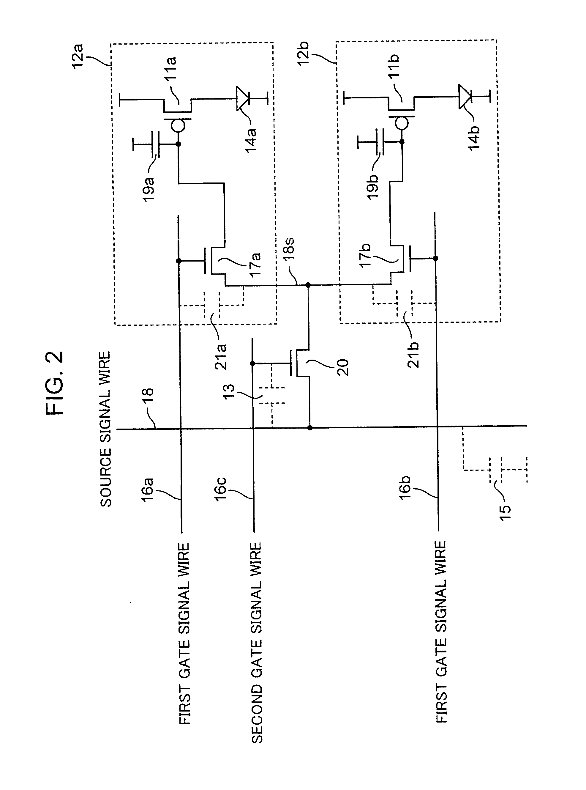
[0056]FIG. 2 is a circuit diagram s...

second embodiment

[0087]In the pixel circuit shown in FIG. 6, the transistor 20 and the switch 17b perform the same behavior. With the switch 17a being in the pixel circuit 12a, it is possible to isolate the voltages stored in the storage capacitances 19a and 19b between the pixel circuit 12a and the pixel circuit 12b. Therefore, in this embodiment, a behavior similar to the second embodiment is performed using a pixel circuit 12c in which the switch 17b is omitted, as shown in FIG. 8.

[0088]Specifically, as shown in FIG. 8, the first gate signal wire 16a and a common gate signal wire 16e are arranged along the row direction of the organic EL panel 3. The first gate signal wire 16a is connected to the pixel circuit 12a. The common gate signal wire 16e is arranged with respect to the pixel circuit 12c. The first gate signal wire 16a and the common gate signal wire 16e are arranged for every row of display pixels. The common gate signal wire 16e is provided with respect to the two pixel circuits 12a and...

third embodiment

[0093]Instead of the circuit configuration shown in FIG. 8, a pixel circuit provided with a switch between drive transistors 11a and 11b and the organic EL elements 14a and 14b may be used. FIG. 9 is a circuit diagram showing the configuration of another pixel circuit applicable to the active matrix display device in the present invention.

[0094]Pixel circuits 12a′ and 12c′ shown in FIG. 9 differ from the pixel circuits 12a and 12c shown in FIG. 8 in that switches 31a and 31b are connected between the drive transistors 11a and 11b and the organic EL elements 14a and 14b, and the gates of the switches 31a and 31b are connected to fifth gate signal wires 16j and 16k, in a similar manner to sixth to eight embodiments described later. Other points are basically similar to the pixel circuits 12a and 12c shown in FIG. 8, and therefore detailed description is omitted.

[0095]FIG. 10 is a timing diagram showing one example of the voltage waveforms of the source signal wire 18, the first gate s...


PUM


Abstract

A display device includes: a plurality of pixel circuits; a first gate signal wire arranged for every two rows of the pixel circuits; a second gate signal wire arranged for every row of the pixel circuits, a source signal wire arranged for every column of the pixel circuits; a switch arranged at each intersection of the second gate signal wire and the source signal wire; and a secondary source signal wire arranged to correspond to each of the switches, each of the pixel circuits including a switch and a storage capacitance, the switch switching between conduction and non-conduction between the source signal wire and the secondary source signal wire in accordance with the voltage of the second gate signal wire, and the switch switching between conduction and non-conduction between the secondary source signal wire and the storage capacitance in accordance with the voltage of the first gate signal wire.

Description

TECHNICAL FIELD[0001]The present invention relates to a display device that displays an image using an organic electro-luminescence element, a liquid crystal element, or the like and a method for driving the same, and particularly relates to an active matrix display device that displays an image pixels using an active element and a method for driving the same.BACKGROUND ART[0002]In an active matrix display device, many display pixels are arranged in a matrix, and an image is displayed by the light intensity being controlled for every pixel in accordance with a picture signal. In recent years, demands for a liquid crystal display device that is an active matrix display device using a liquid crystal element are increasing due to advantages such as light weight, thinness, and low power consumption. In order to achieve light weight, thinness, low power consumption, and the like further, an active matrix display device using an organic electro-luminescence element (hereinafter, abbreviat...

Claims


Application Information

Patent Timeline
IPC IPC(8): G09G3/32
CPCG09G3/3233G09G2300/0804G09G2300/0814G09G2300/0842G09G2300/0861G09G2310/0205G09G2310/0208G09G3/3208
Inventor TSUGE, HITOSHI
Owner JOLED INC
Learn More