Antenna, transmitter device, receiver device, three-dimensional integrated circuit, and contactless communication system

Active Publication Date: 2014-10-30
PANASONIC INTELLECTUAL PROPERTY MANAGEMENT CO LTD
View PDF39 Cites 67 Cited by
  • Summary
  • Abstract
  • Description
  • Claims
  • Application Information

AI Technical Summary

Benefits of technology

[0011]The antenna according to one aspect of the present invention includes the at least two antenna elements connecting the first and second junctions. Even when each of the antenna elements consists of a wiring line of severely reduced width, the resistance between the two junctions can be reduced to a sufficiently low le

Problems solved by technology

On the other hand, TSVs have too fine structures to easily achieve a more

Method used


Image

  • Antenna, transmitter device, receiver device, three-dimensional integrated circuit, and contactless communication system
  • Antenna, transmitter device, receiver device, three-dimensional integrated circuit, and contactless communication system
  • Antenna, transmitter device, receiver device, three-dimensional integrated circuit, and contactless communication system

Examples


embodiment 1

Merits of Embodiment 1

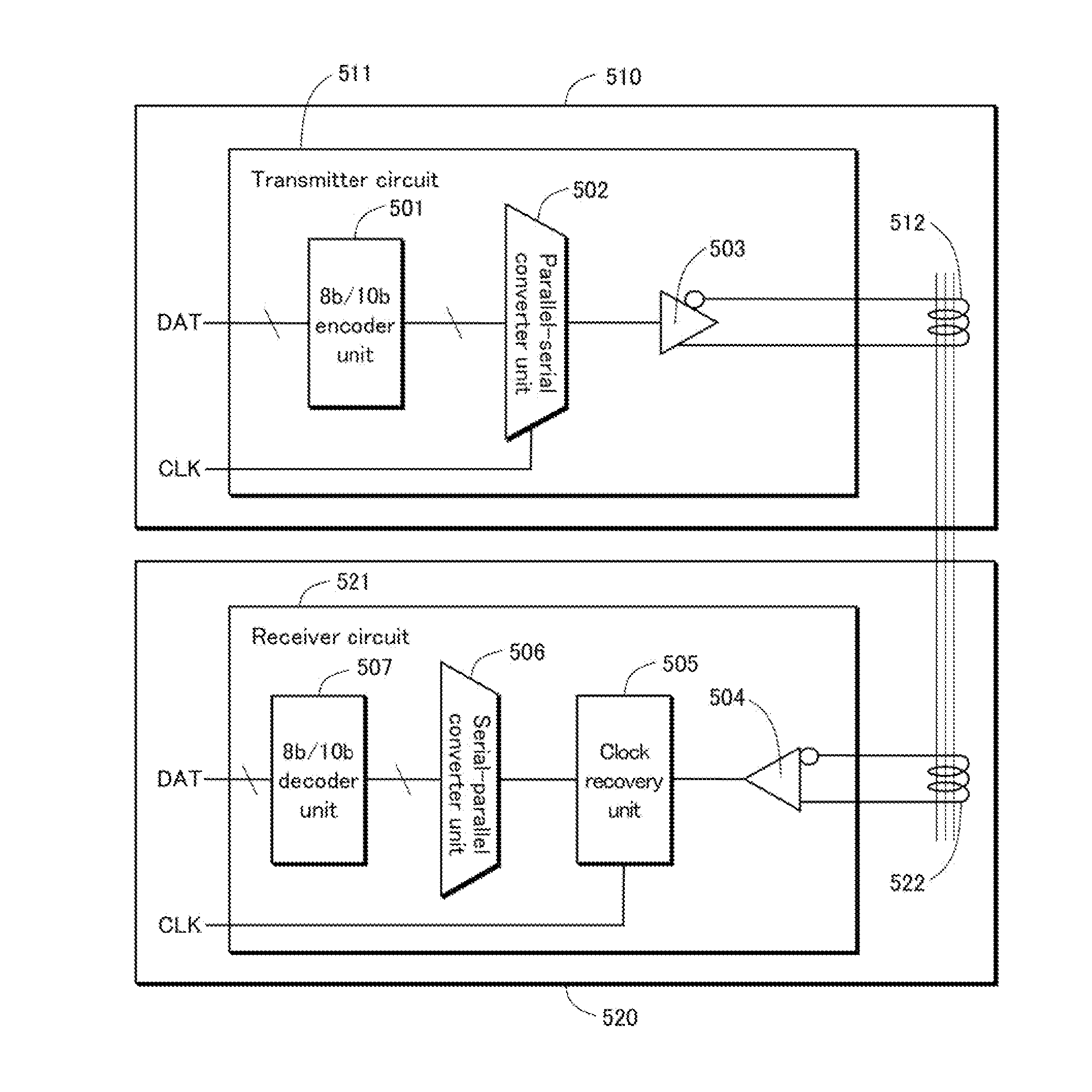
[0037]FIG. 6 includes plan views of a coil antenna including only one antenna element (hereinafter referred to as a “first coil antenna”) and the coil antenna shown in FIG. 3 (hereinafter referred to as a “second coil antenna”), and gain-frequency characteristic graphs of the first and second coil antennas. Referring to FIG. 6, the first coil antenna 600 includes a first terminal 601, a second terminal 602, and a single antenna element 611. The first and second terminals 601, 602 receive a differential signal from the communication circuit 113 on the same chip. The antenna element 611, like the two elements 311, 312 shown in FIG. 3, consists of a wiring line on the chip, and is a substantially rectangular spiral. The first and second coil antennas 600, 300 are similar to each other such that: the wiring lines composing the first and second coil antennas 600, 300 have the same width; the distance between turns of the wiring line composing the first coil antenna ...

embodiment 2

[0056]FIG. 16 is a schematic view of a contactless communication system according to Embodiment 2 of the present invention. Referring to FIG. 16, this system includes a first chip 1610 built in a cellular phone CPH and a second chip 1620 built in a cradle CRD. This system is used for data exchange between the cellular phone CPH and the cradle CRD.

[0057]The first chip 1610 is located near a surface of the body of the cellular phone CPH, and includes a first coil antenna 1611 and a first transceiver circuit 1612. The first coil antenna 1611 consists of wiring lines on the first chip 1610. The first coil antenna 1611 is connected via a wiring layer of the first chip 1610 (not shown in FIG. 16) with the first transceiver circuit 1612. The first coil antenna 1611 has a shape similar to that of the coil antenna 300 shown in FIG. 3, and in particular, has two antenna elements running parallel between ends of the first coil antenna 1611. The two antenna elements form concentric spirals. The...


PUM


Abstract

A system including a device with a first chip and a device with a second chip, to realize contactless communication therebetween. The first chip includes a transmitter circuit converting parallel data into a differential signal and a transmitting antenna transmitting the signal to the second chip. The second chip includes a receiving antenna receiving the differential signal from the transmitting antenna and a receiver circuit converting the differential signal into the parallel data. The transmitting and receiving antenna each include at least two antenna elements, first and second terminals, and first and second junctions. The antenna elements consist of wiring lines on the chips. The terminals are connected with circuits on the chips. At the first junction, first ends of the antenna elements meet to connect to the first terminal. At the second junction, second ends of the antenna elements meet to connect to the second terminal.

Description

TECHNICAL FIELD[0001]The present invention relates to contactless communication technologies, in particular, to their application to chip-to-chip communication in three-dimensional integrated circuits.BACKGROUND ART[0002]Contactless communication is a technology for wireless communication with an extremely-short range of up to 10 centimeters. Contactless communication is used in, for example, communication between IC cards and automatic ticket gates, communication between IC cards or mobile phones and automatic vending machines or electric cash registers, communication between IC cards and security systems, and electric power transmission to mobile devices such as cellular phones. Technologies of applying contactless communication are more recently being developed for use in chip-to-chip communication in three-dimensional integrated circuits, in addition to keyless entry for cars, data exchange between mobile devices and personal computers, and the likes.[0003]Three-dimensional inte...

Claims


Application Information

Patent Timeline
IPC IPC(8): H01Q7/00H01Q21/00
CPCH01Q7/00H01Q21/00H01Q1/2283H01L2224/16225H01L2224/32145H01L2224/73253H01L2924/15311H01L23/5227H01L23/66H01L25/0657H01L2223/6677H01L2225/06531
Inventor ASAI, KOJINAKAYAMA, TAKESHI
Owner PANASONIC INTELLECTUAL PROPERTY MANAGEMENT CO LTD
Why Eureka
Try Eureka