Manufacturing method of power semiconductor

a manufacturing method and technology of power semiconductor, applied in the direction of semiconductors, electrical devices, transistors, etc., can solve the problems of unlimited characteristics of power semiconductors, reduce the processing efficiency of power semiconductors, limit the melting point of surface metals, etc., to achieve the effect of reducing the drawbacks of phenomenon, reducing the thickness of wafers, and reducing the processing efficiency

Active Publication Date: 2014-11-06
MOSEL VITELIC INC
View PDF0 Cites 0 Cited by
  • Summary
  • Abstract
  • Description
  • Claims
  • Application Information

AI Technical Summary

Benefits of technology

[0007]The present invention provides a manufacturing method of a power semiconductor in order to eliminate the drawbacks of the phenomenon caused by thinning the wafer thickness, the limitation of the melting point of the surface metal, the low process flexibility, and the limitation of the characteristics of power semiconductors.
[0008]The present invention also provides a manufacturing method of a power semiconductor. By respectively fabricating a first semiconductor substrate and a second semiconductor substrate and forming a third semiconductor substrate by combining the first semiconductor substrate and the second semiconductor substrate, a N-type buffer layer and a P-type injection layer are formed through ion implanting and high-temperature drive-in diffusion, which are not limited by the melting point of the metal. As a result, the process flexibility is enhanced, and the characteristics of the power semiconductor are un-limited.
[0009]The present invention further provides a manufacturing method of a power semiconductor. Since a first semiconductor substrate is carried on and combined with a fourth semiconductor substrate, the phenomenon of easily bending and frangibility caused by thinning the wafer thickness is avoided, and the backside implant process and the backside anneal process are smoothly proceeded.

Problems solved by technology

As a result, the process flexibility is enhanced, and the characteristics of the power semiconductor are un-limited.

Method used


Image

  • Manufacturing method of power semiconductor
  • Manufacturing method of power semiconductor
  • Manufacturing method of power semiconductor

Examples


Embodiment Construction

[0016]The present invention will now be described more specifically with reference to the following embodiments. It is to be noted that the following descriptions of preferred embodiments of this invention are presented herein for purpose of illustration and description only. It is not intended to be exhaustive or to be limited to the precise form disclosed.

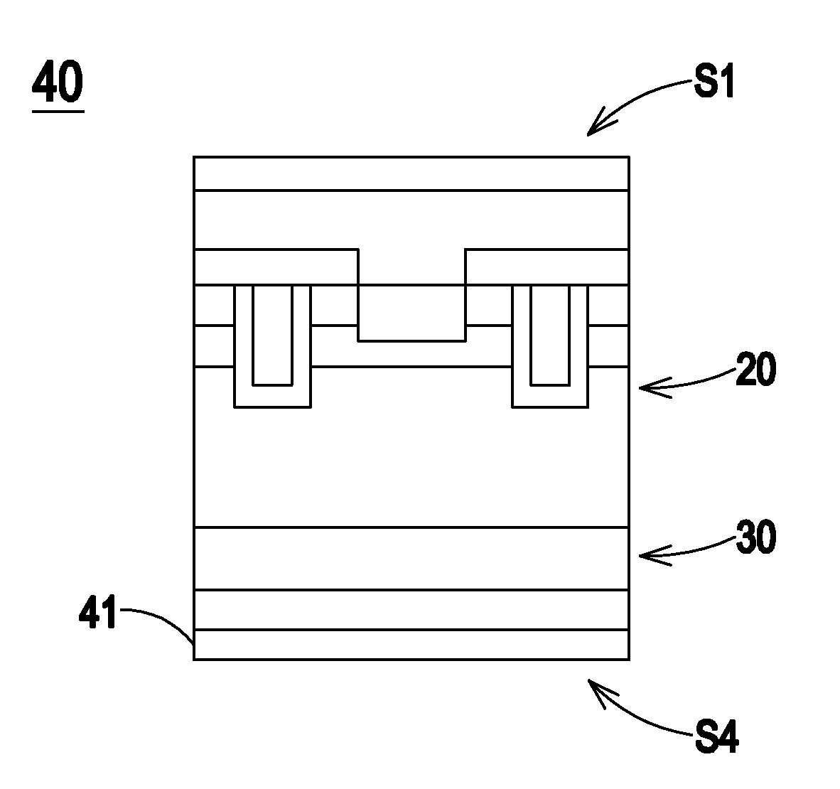
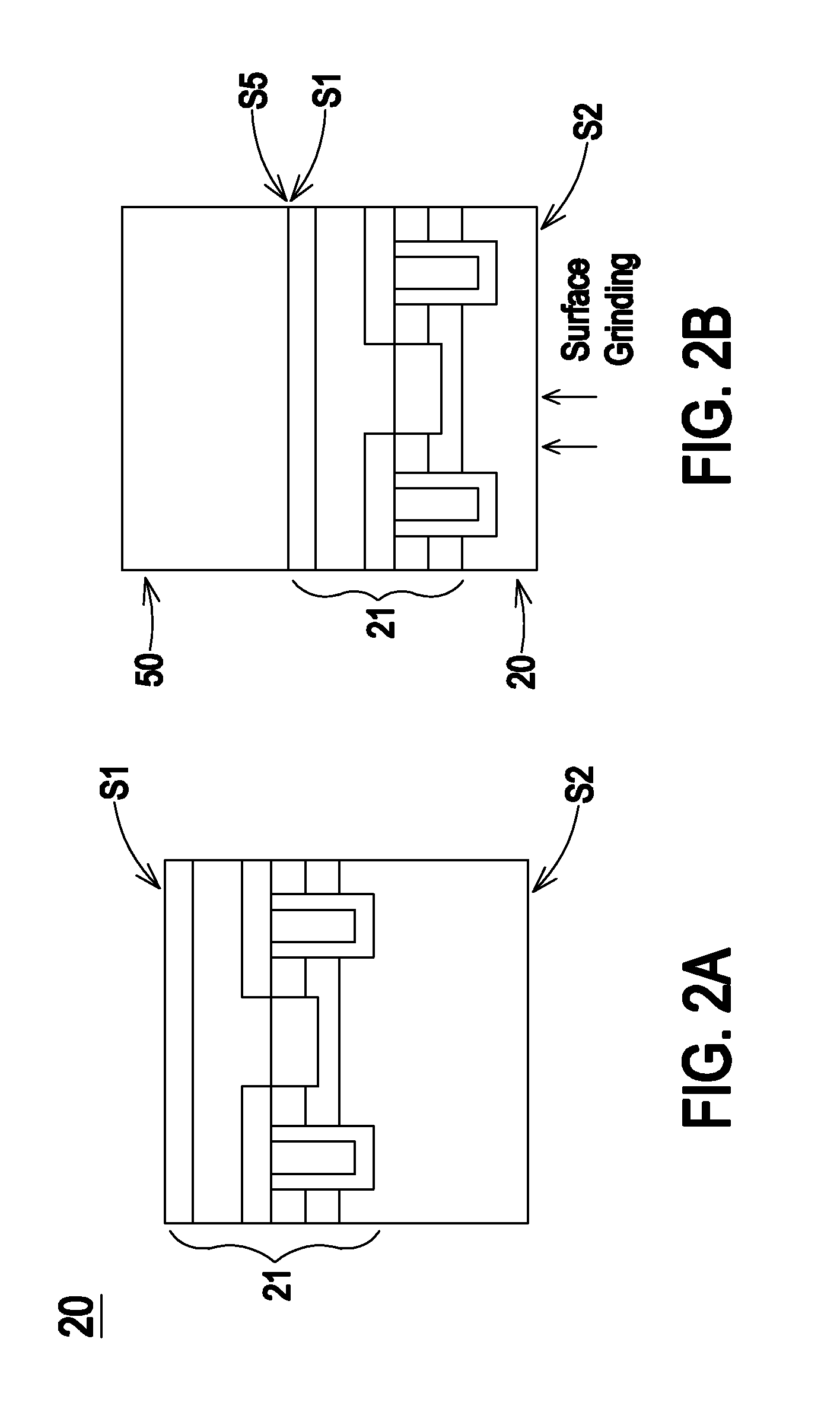
[0017]Please refer to FIG. 2A to FIG. 2GFIG. 2A to FIG. 2G schematically illustrate the structures corresponding to the steps of a manufacturing method of a power semiconductor according to an embodiment of the present invention. A manufacturing method of a power semiconductor of the present invention includes steps as following. First, as shown in FIG. 2A and FIG. 2C, providing a first semiconductor substrate 20 and a second semiconductor substrate 30, among which the first semiconductor substrate 20 is not limited to a N-type semiconductor wafer made of a N-type floating zone substrate, and the first semiconductor substrate 20 ...


PUM


Abstract

A manufacturing method of a power semiconductor includes steps of providing a first semiconductor substrate and a second semiconductor substrate, forming a metal oxide semiconductor layer on a first surface of the first semiconductor substrate, grinding a second surface of the first semiconductor substrate, forming a N-type buffer layer and a P-type injection layer on a third surface of the second semiconductor substrate through ion implanting, grinding a fourth surface of the second semiconductor substrate, and combining the second surface of the first semiconductor substrate with the third surface of the second semiconductor substrate for forming a third semiconductor substrate. As a result, the present invention achieves the advantages of enhancing the process flexibility and un-limiting the characteristics of the power semiconductor.

Description

FIELD OF THE INVENTION[0001]The present invention relates to a manufacturing method of a semiconductor, and more particularly to a manufacturing method of a power semiconductor using multiple wafer bonding technology.BACKGROUND OF THE INVENTION[0002]In recent years, with the growing of the technologies, lot types of electronic products are produced. The high-tech electronic devices are deeply combined with human's daily life. For example, each of the panels and the global positioning systems of automobiles, smart phones, tablet PCs, variety toys and remote-controlled apparatuses is part of the technology life of human nowadays. The mainly necessary elements in electronic devices are semiconductor elements, such like power semiconductors, transistors, amplifiers and switches, especially the power semiconductors are much more fabricated in industry.[0003]For example, one of the common power semiconductors is an insulated gate bipolar transistor (hereinafter “IGBT”). The basic encapsul...

Claims


Application Information

Patent Timeline
Patent Type & Authority Applications(United States)
IPC IPC(8): H01L29/66
CPCH01L29/66333H01L21/187H01L21/6835H01L29/66348H01L2221/68327H01L2221/6834
Inventor CHANG, CHIEN-PING
Owner MOSEL VITELIC INC
Why Eureka
Try Eureka