Multiple pixel surface mount device package

a surface mount device and multi-pixel technology, applied in the field of light-emitting diode packages and displays, can solve the problems of increasing the complexity of the interconnection between the display and the display, and achieve the effects of simplifying the design and manufacturing of displays, reducing the cost, and reducing the cost per pixel

Active Publication Date: 2014-12-04
CREE HUIZHOU SOLID STATE LIGHTING
View PDF18 Cites 50 Cited by
  • Summary
  • Abstract
  • Description
  • Claims
  • Application Information

AI Technical Summary

Benefits of technology

[0011]The present invention is directed to emitter packages and LEDs displays utilizing the packages, with the packages arranged to reduce the cost and interconnect complexity for the displays. Some pa...

Problems solved by technology

As the number of pixels increases, the interconnect complexity for the display also increases.
This interconnect complexity can be one of the maj...

Method used


Image

  • Multiple pixel surface mount device package
  • Multiple pixel surface mount device package
  • Multiple pixel surface mount device package

Examples


Embodiment Construction

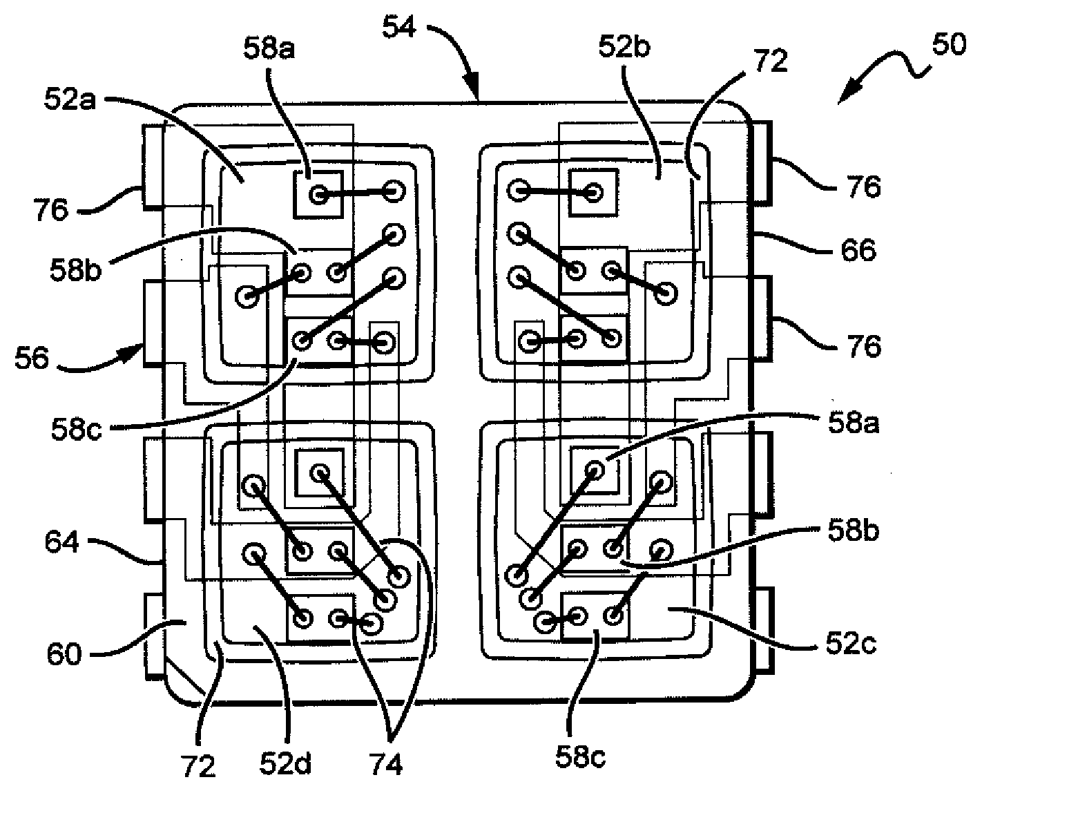
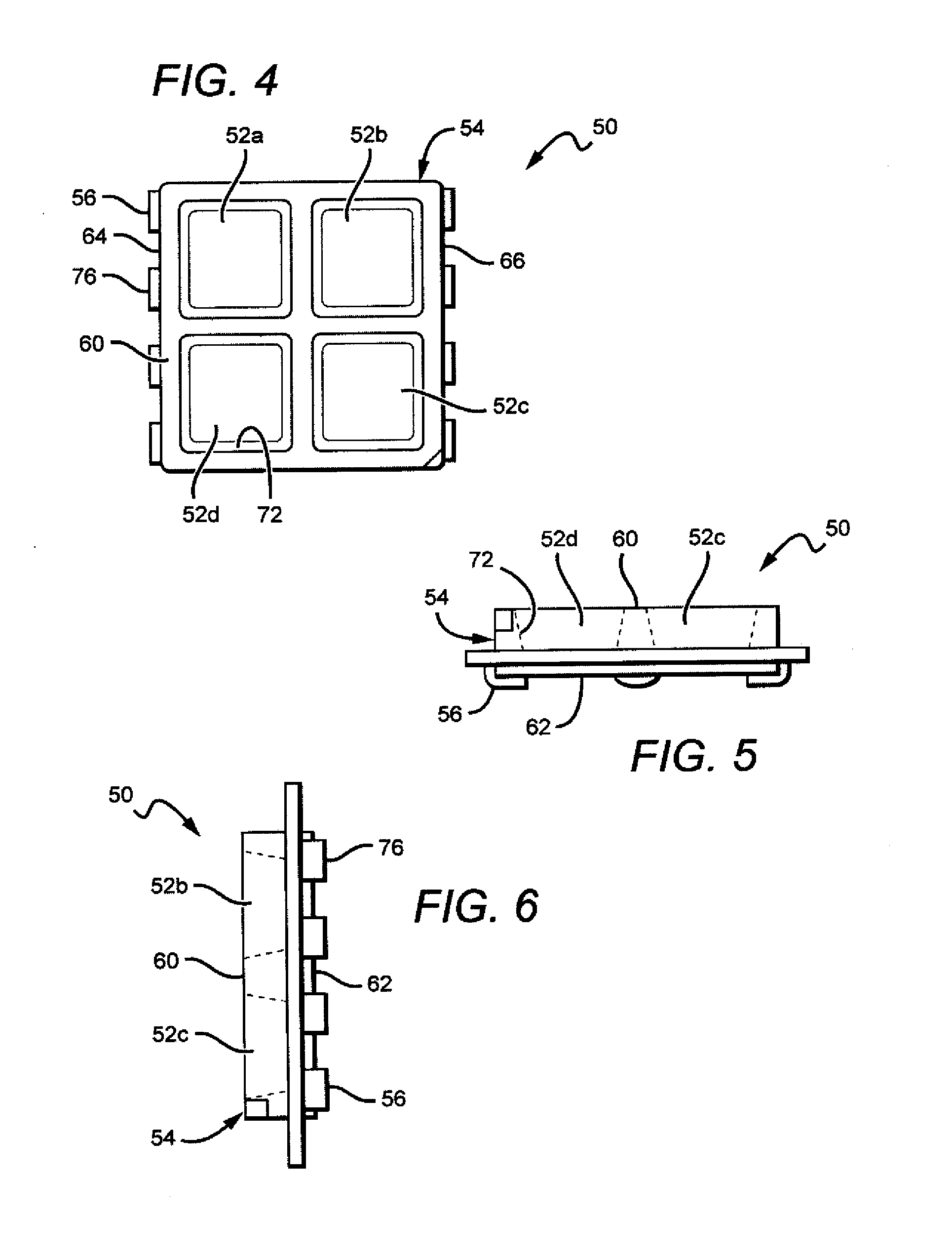
[0043]The present invention is directed to improved LED packages and LED displays utilizing the LED packages, with the LED packages according to the present invention comprising “multiple pixel” packages. That is, the packages comprise more than one pixel, with each of the pixels comprising one or more light emitting diodes. The different embodiments comprise different features for applying an electrical signal to the LED in the pixels. In some embodiments, a respective electrical signal can be applied to each of the pixels to control its emission color and / or intensity, while in other embodiments two or more of the pixels can be controlled by the same electrical signal. In embodiments where the pixels have multiple LEDs one or more of the LEDs in each pixel can be controlled by respective signals, while in other embodiments the LEDs in different pixels can be controlled by the same signal. In some of these embodiments, the same signal can be used to control the emission of two or m...


PUM


Abstract

Emitter packages and LEDs displays utilizing the packages are disclosed, with the packages providing advantages such as reducing the cost and interconnect complexity for the packages and displays. One emitter package comprises a casing with a plurality of cavities, each cavity having at least one LED. A lead frame structure is included integral to the casing, with the at least one LED from each of the cavities mounted to the lead frame structure. The package is capable of receiving electrical signals for independently controlling the emission from a first and second of the cavities. One LED display utilizes the LED packages mounted in relation to one another to generate a message or image. The LED packages comprise multiple pixels each having at least one LED, with each package capable of receiving electrical signals for independently controlling the emission of at least a first and second of the pixels.

Description

BACKGROUND OF THE INVENTION[0001]1. Field of the Invention[0002]This invention relates to light emitting diode packages and displays utilizing light emitting diode packages as their light source.[0003]2. Description of the Related Art[0004]Light emitting diodes (LED or LEDs) are solid state devices that convert electric energy to light, and generally comprise one or more active layers of semiconductor material sandwiched between oppositely doped layers. When a bias is applied across the doped layers, holes and electrons are injected into the active layer where they recombine to generate light. Light is emitted from the active layer and from all surfaces of the LED.[0005]Technological advances over the last decade or more has resulted in LEDs having a smaller footprint, increased emitting efficiency, and reduced cost. LEDs also have an increased operation lifetime compared to other emitters. For example, the operational lifetime of an LED can be over 50,000 hours, while the operation...

Claims


Application Information

Patent Timeline
IPC IPC(8): H01L27/15
CPCH01L27/156H01L24/97H01L25/0753H01L33/50H01L2224/48091H01L2224/48247H01L2924/12041H01L2924/00014H01L2924/00H01L33/62
Inventor PANG, CHAK HAU CHARLESCHAN, CHI KEUNG ALEXEMERSON, DAVIDLAU, YUE KWONG VICTORZHONG, ZHANYU
Owner CREE HUIZHOU SOLID STATE LIGHTING
Why Eureka
Try Eureka