Organic light-emitting display panel

Active Publication Date: 2014-12-04
SAMSUNG DISPLAY CO LTD
View PDF10 Cites 62 Cited by
  • Summary
  • Abstract
  • Description
  • Claims
  • Application Information

AI Technical Summary

Benefits of technology

[0027]According to an exemplary embodiment of the present invention, an organic light-emitting display panel includes a pixel unit connected to a plurality of scanning lines and a plurality of data lines, and including a plurality of pixels, a panel test unit connected to first ends of the plurality of data lines, and configured to output a panel test signal for testing the plurality of pixels, a plurality of data pads connected to second ends of the plurality of data lines, and an array test unit configured to selectively apply a plurality of array test signals to a pixel column of the pixel unit according to a plurality of array test control signals, and detect a signal output from the pixel column to which the plurality of array test signals are applied.
[0028]According to an exemplary embodiment of the present invention, an organic light-emitting display panel includes a plurality of array test pads configured to contact a probe pin of an array test apparatus and receive an array test signal, and a demultiplexer disposed between a plurality of data pads and the plurality of array test pads, and configured to selectively apply the array test signal to a pixel column of a pixel unit via the plurality of data pads according to a plurality of array tes

Problems solved by technology

As a result, a process of manufacturing the organic light-emitting display apparatus may be complicated, and the reliability of the final product and the yield of the

Method used


Image

  • Organic light-emitting display panel
  • Organic light-emitting display panel
  • Organic light-emitting display panel

Examples


Example

[0037]Exemplary embodiments of the present invention will be described more fully hereinafter with reference to the accompanying drawings. Like reference numerals may refer to like elements throughout the accompanying drawings.

[0038]It will be understood that the terms “includes,” and / or “including,” when used herein, specify the presence of components, but do not preclude the presence or addition of one or more other components. Additionally, when an object is referred to as being “on” another object, the object can be located above or below another object, and the object may be located directly or indirectly on another object.

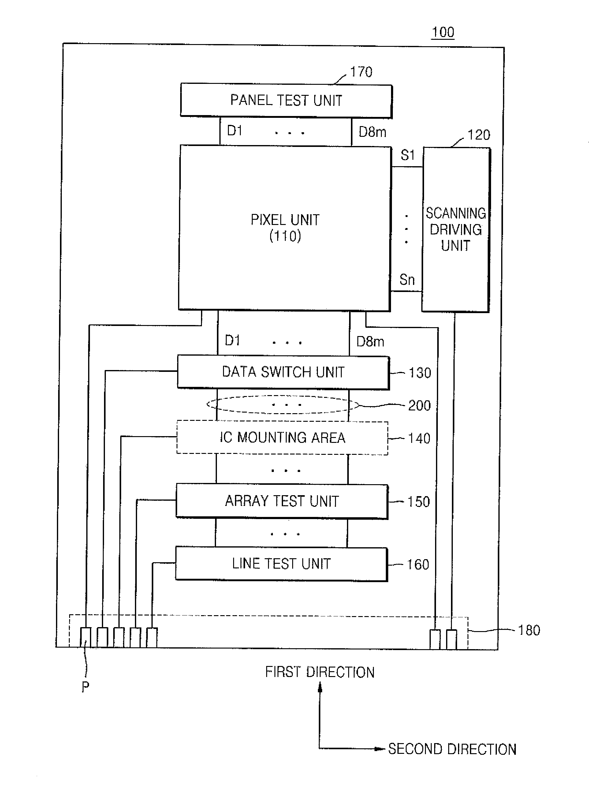
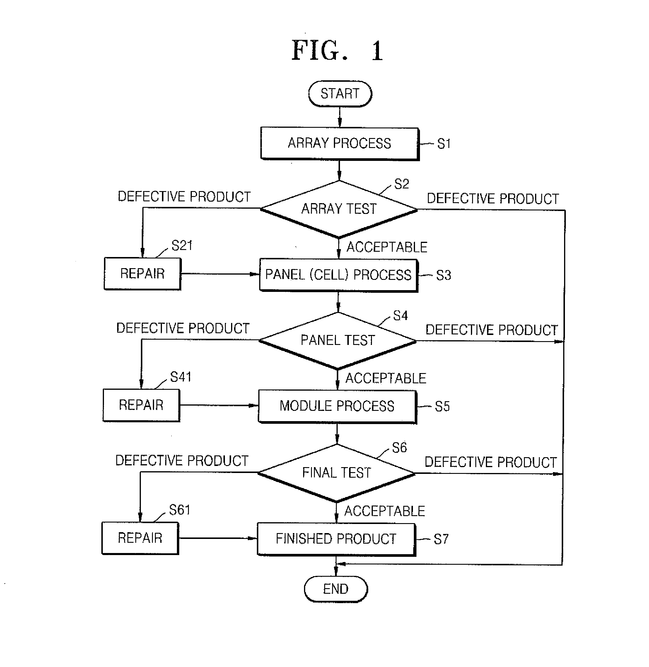
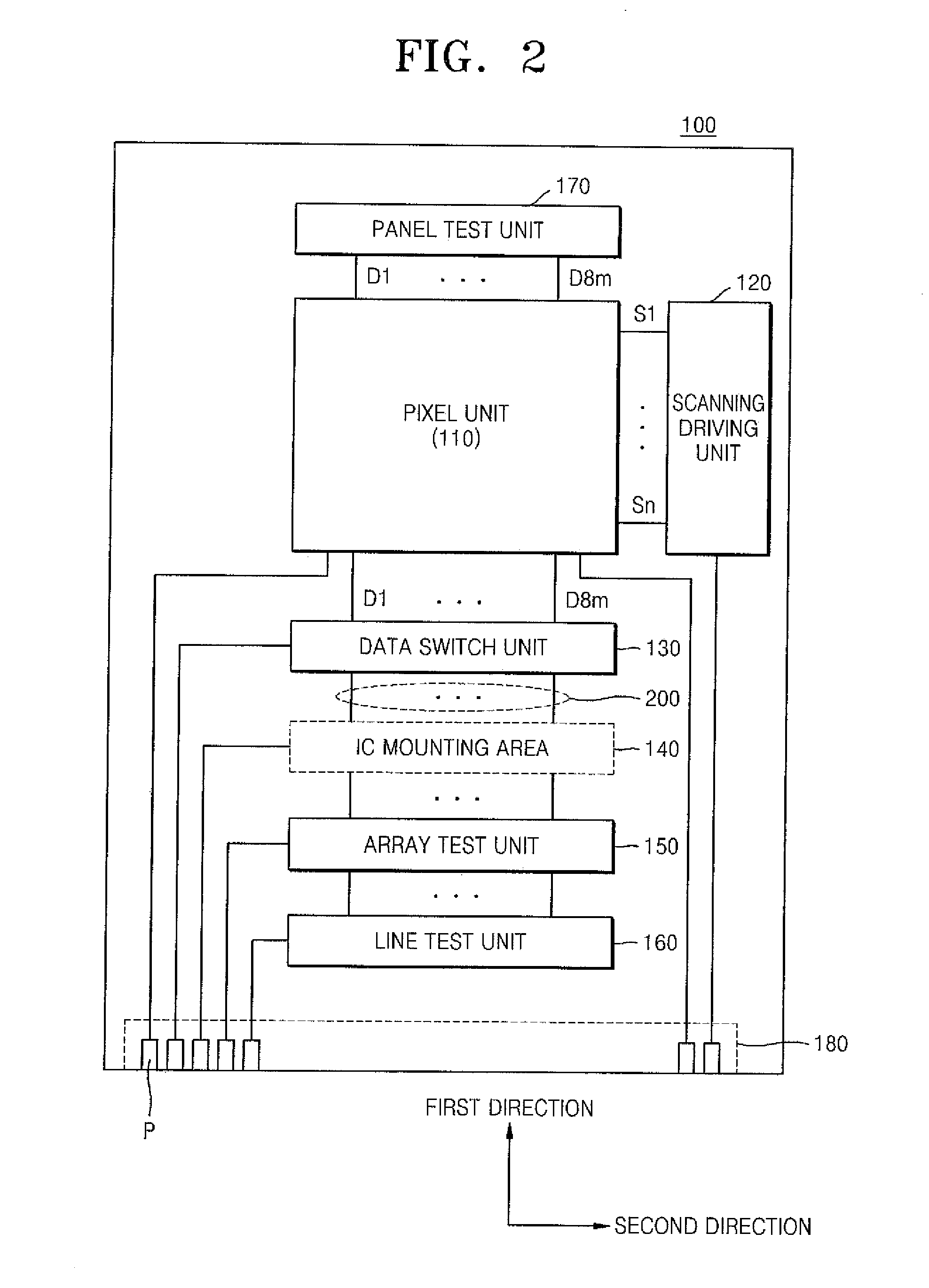
[0039]FIG. 1 is a flowchart illustrating a method of manufacturing an organic light-emitting display apparatus, according to an exemplary embodiment of the present invention.

[0040]At operation S1, an array process that forms a pixel circuit array on a substrate is performed. A pixel circuit in the pixel circuit array may include, for example, two or more thin...


PUM


Abstract

An organic light-emitting display panel includes a pixel unit connected to a plurality of scanning lines and a plurality of data lines, and including a plurality of pixels, a panel test unit connected to first ends of the plurality of data lines, and configured to output a panel test signal for testing the plurality of pixels, a plurality of data pads connected to second ends of the plurality of data lines, and an array test unit configured to selectively apply a plurality of array test signals to a pixel column of the pixel unit according to a plurality of array test control signals, and detect a signal output from the pixel column to which the plurality of array test signals are applied.

Description

CROSS-REFERENCE TO RELATED PATENT APPLICATIONS[0001]This application claims priority under 35 U.S.C. §119 to Korean Patent Application No. 10-2013-0063078, filed on May 31, 2013, the disclosure of which is incorporated by reference herein in its entirety.TECHNICAL FIELD[0002]Exemplary embodiments of the present invention relate to an organic light-emitting display panel.DISCUSSION OF THE RELATED ART[0003]An organic light-emitting display apparatus displays an image by using a self-emission device such as an organic light-emitting diode. Due to its excellent brightness and color purity, use of the organic light-emitting display apparatus is increasing.[0004]During manufacture of an organic light-emitting display apparatus, a tape-automated bonding (TAB) method may be used to connect a high-density integrated circuit (IC), including a driving circuit that generates and applies a scanning signal and a data signal to a pixel, to an array substrate that includes a plurality of pixels. In...

Claims


Application Information

Patent Timeline
IPC IPC(8): G09G3/00
CPCG09G3/006G09G3/3225G09G2300/0852G09G3/30H01L22/12H10K59/121H10K59/122
Inventor KIM, JI-HYE
Owner SAMSUNG DISPLAY CO LTD
Why Eureka
Try Eureka