
Display device and display method

a display device and display method technology, applied in static indicating devices, instruments, electroluminescent light sources, etc., can solve the problems of large voltage swing of video signal outputted by liquid crystal panel drivers, display defects, and high power consumption, so as to reduce power consumption of driving video signal lines, and reduce the effect of video signal lines

Inactive Publication Date: 2014-12-25
SHARP KK
View PDF3 Cites 15 Cited by
  • Summary
  • Abstract
  • Description
  • Claims
  • Application Information

AI Technical Summary

Benefits of technology

The technical effects of this patent include reducing power consumed by driving video signal lines by selectively driving certain scanning signal lines based on their potential for variation and minimizing the integral of potential variation caused by changes in video signal lines. Additionally, minimizing power consumption may be achieved by selecting the first scanning signal line to display an image based on its potential for variation and subsequently selecting the next scanning signal line accordingly. This approach helps to significantly reduce power consumption even in situations where potentials applied to video signal lines remain unchanged.

Problems solved by technology

However, this drive scheme is subject to display defects, such as flicker, upon display, and therefore, in the drive schemes employed in recent years, the polarity of an applied voltage is inverted every horizontal scanning line and also every frame (a so-called “line inversion drive scheme”) or the polarity of an applied voltage is inverted every two vertically / horizontally adjacent pixels and also every frame (a so-called “dot inversion drive scheme”).
The dot inversion drive scheme is less prone to the occurrence of flicker, so that high-quality display can be achieved, but the polarity of a video signal to be applied to the liquid crystal panel is switched between predetermined voltages respectively above and below the potential of the common electrode, and therefore, the voltage swing of a video signal outputted by a liquid crystal panel driver is large, so that power consumption tends to be high.
However, even when such a drive scheme is employed, the potentials of video signals might change significantly depending on the image to be displayed, which results in a large voltage swing, so that power consumption tends to become high.

Method used


Image

  • Display device and display method
  • Display device and display method
  • Display device and display method

Examples


first embodiment

1. First Embodiment

1.1 Overall Configuration and Operation of the Liquid Crystal Display Device

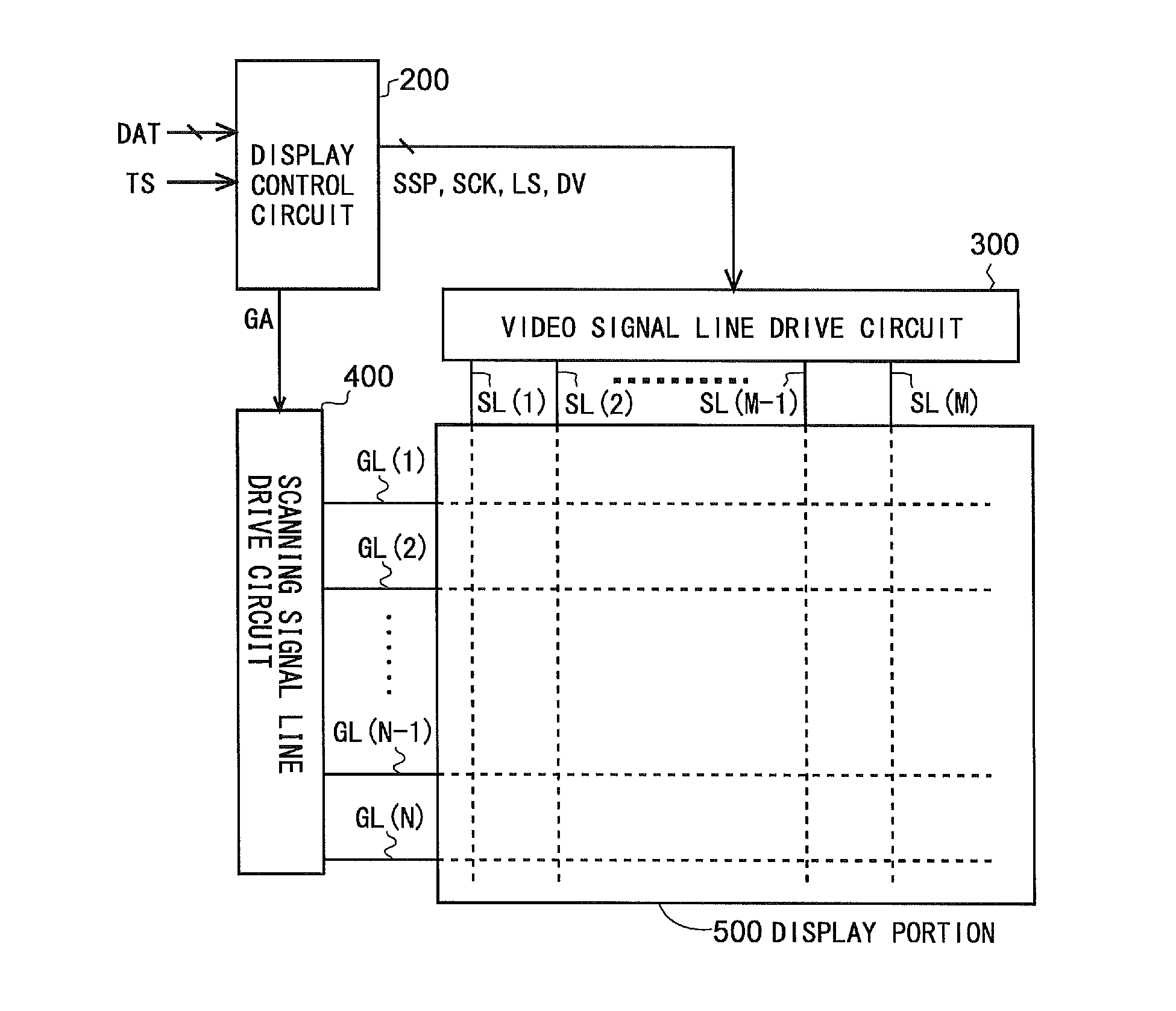
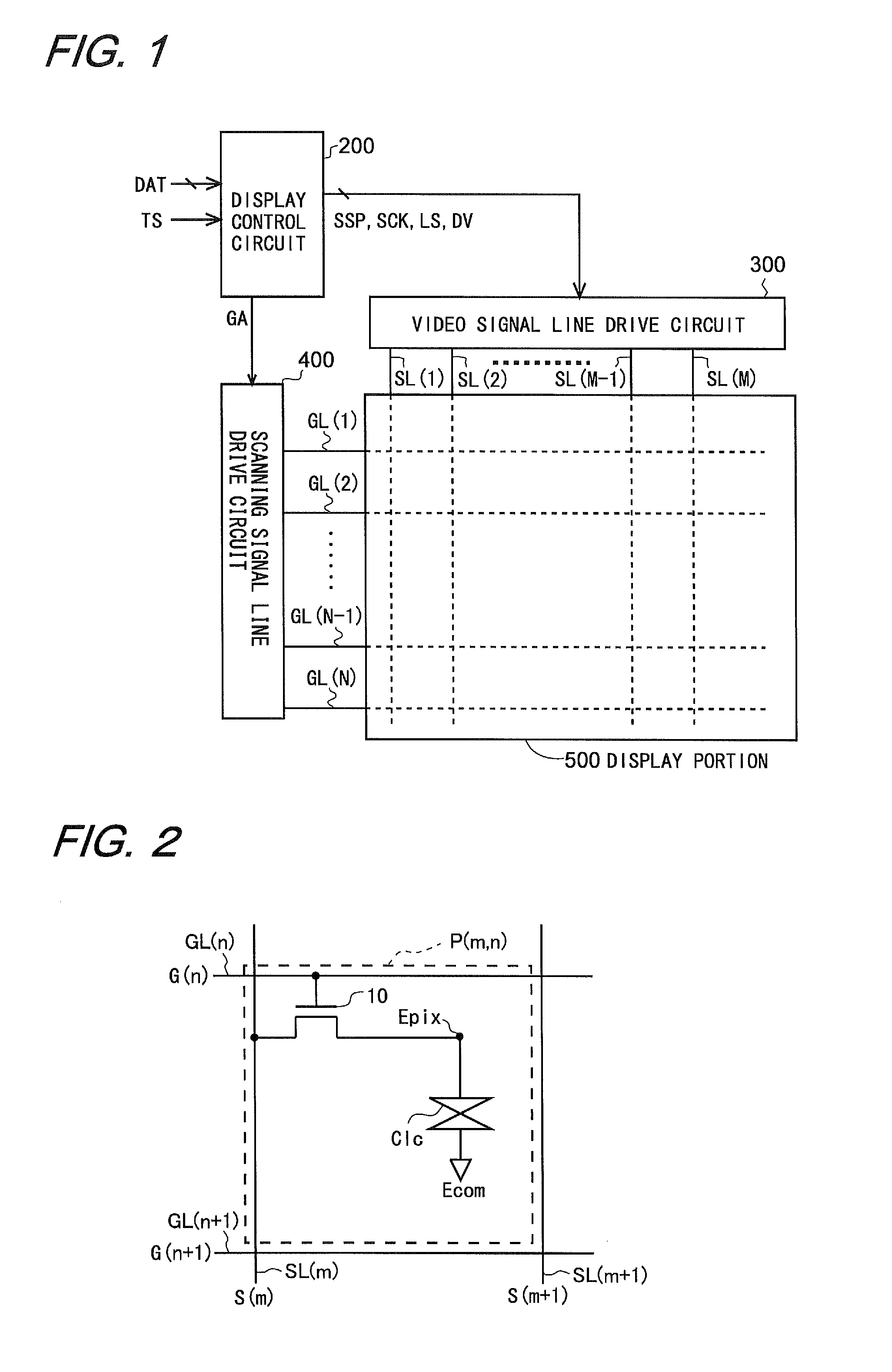
[0067]FIG. 1 is a block diagram illustrating the overall configuration of an active-matrix liquid crystal display device according to a first embodiment of the present invention. This liquid crystal display device includes a drive control portion consisting of a display control circuit 200, a video signal line drive circuit (source driver) 300, and a scanning signal line drive circuit (gate driver) 400, as well as a display portion 500. The display portion 500 includes a plurality (M) of video signal lines SL(1) to SL(M), a plurality (N) of scanning signal lines GL(1) to GL(N), and a plurality (M×N) of pixel forming portions provided along the video signal lines SL(1) to SL(M) and the scanning signal lines GL(1) to GL(N). Note that in the following, a pixel forming portion provided in association with and in the vicinity (in the figure, to the lower right) of the intersection of a scanning...

second embodiment

2. Second Embodiment

2.1 Overall Configuration and Operation of the Liquid Crystal Display Device

[0113]An active-matrix liquid crystal display device according to the present embodiment has the same configuration as the display device of the first embodiment shown in FIG. 1, except for a part of the display control circuit, and also operates in the same manner, therefore, the same components will be denoted by the same characters, and any descriptions thereof will be omitted.

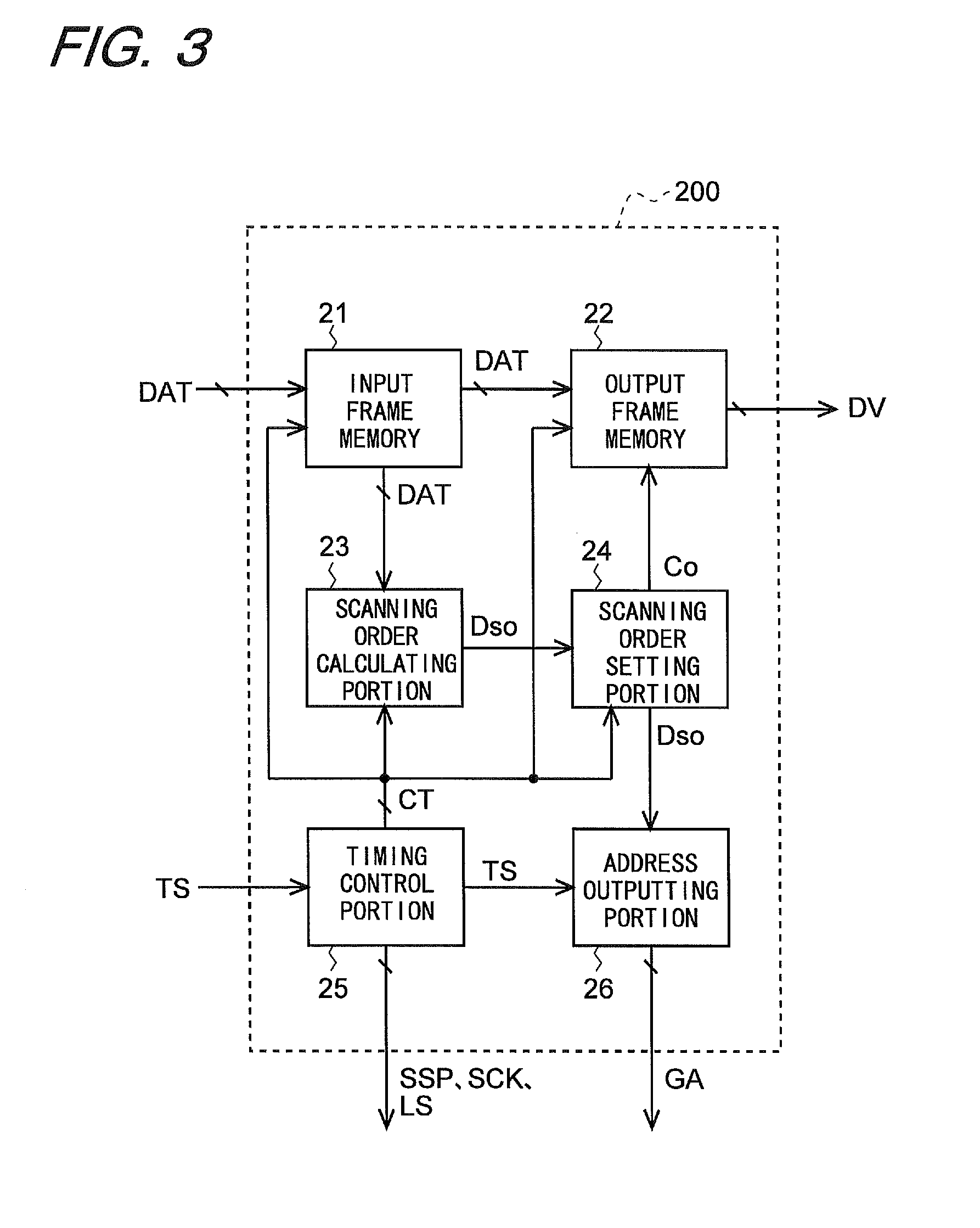
[0114]FIG. 10 is a block diagram illustrating the configuration of the display control circuit in the second embodiment of the present invention. As can be appreciated in comparison with the display control circuit 200 shown in FIG. 3, the display control circuit 210 shown in FIG. 10 operates in the same manner and has the same configuration except that a display transition detecting portion 28 is additionally provided, therefore, the same components are denoted by the same characters, and any descriptions thereo...

third embodiment

3. Third Embodiment

3.1 Overall Configuration and Operation of the Liquid Crystal Display Device

[0123]An active-matrix liquid crystal display device according to the present embodiment has the same configuration as the display device of the first embodiment shown in FIG. 1, except for a part of the display control circuit, and also operates in the same manner, therefore, the same components will be denoted by the same characters, and any descriptions thereof will be omitted.

[0124]FIG. 13 is a block diagram illustrating the configuration of the display control circuit in the third embodiment of the present invention. As can be appreciated in comparison with the display control circuit 200 shown in FIG. 3, the display control circuit 230 shown in FIG. 13 operates in the same manner and also has the same configuration except that output line memory 32 is provided in place of the output frame memory 22, an intra-block scanning order calculating portion 33 is provided in place of the scan...


PUM


Abstract

A scanning order calculating portion (23) included in a display control circuit (200) determines the order of selecting all rows by repeating the following: the row for which the total amount of potential variation relative to a reference row is the lowest is selected as a subsequent row, and the row having been selected as the subsequent row is used as the next reference row in a similar operation to determine the next row to be set as a subsequent row. A scanning order setting portion (24) controls an address outputting portion (26) such that the scanning signal lines are selected in the determined order, and also controls digital image signals DV outputted by output frame memory (22). Power consumed by driving video signal lines can be reduced by selecting the scanning signal lines in such an order that the total amount of potential variation of the video signal lines becomes smaller.

Description

TECHNICAL FIELD[0001]The present invention relates to display devices, more specifically to an active-matrix display device and a display method in which the order of scanning is changed.BACKGROUND ART[0002]In general liquid crystal display devices, polarity inversion drive is performed in order to suppress liquid crystal deterioration. A known polarity inversion drive scheme is a scheme (frame inversion drive scheme) in which the polarity of a voltage applied to the liquid crystal is inverted every frame. However, this drive scheme is subject to display defects, such as flicker, upon display, and therefore, in the drive schemes employed in recent years, the polarity of an applied voltage is inverted every horizontal scanning line and also every frame (a so-called “line inversion drive scheme”) or the polarity of an applied voltage is inverted every two vertically / horizontally adjacent pixels and also every frame (a so-called “dot inversion drive scheme”).[0003]The dot inversion dri...

Claims


Application Information

Patent Timeline
Patent Type & Authority Applications(United States)
IPC IPC(8): G09G3/36H05B44/00
CPCG09G3/3674G09G3/3225G09G3/3614G09G2310/0224G09G2320/0219G09G3/2092
Inventor NAKAGAWA, YOUSUKEMAEDA, KAZUHIRO
Owner SHARP KK
Learn More