Liquid crystal display panel and liquid crystal display device

a liquid crystal display panel and liquid crystal display technology, applied in the field of liquid crystal display techniques, can solve the problems of color distortion at large viewing angle, difficulty in controlling the gamma curve of the two pixel area, and low color shift, so as to reduce the problem of image retention, reduce the different colors, and improve the effect of low color shi

Inactive Publication Date: 2015-01-01
SHENZHEN CHINA STAR OPTOELECTRONICS TECH CO LTD
View PDF7 Cites 13 Cited by
  • Summary
  • Abstract
  • Description
  • Claims
  • Application Information

AI Technical Summary

Benefits of technology

[0027]The efficacy of the present invention is that to be distinguished from the state of the art. In the liquid crystal display panel according to the present invention, each pixel unit in the first substrate comprises the first pixel electrode and the second pixel electrode, and the corresponding charging scan line and data line of the pixel unit drive the first pixel electrode and the second pixel electrode to display through the first switch and the second switch; the third switch is connected to the corresponding discharging scan line of the pixel unit; the input terminal of the third switch is connected to the first pixel electrode or the second pixel electrode; the output terminal of the third switch is connected to the discharging circuit; when driving the first pixel electrode and the second pixel electrode to display, the effect of the discharging circuit makes a non-zero default voltage difference formed between the first pixel electrode and the second pixel electrode. In other words, the voltage at the first pixel electrode is different from the voltage at the second pixel electrode, which leads to the result that the orientation of the liquid crystal molecules of the liquid crystal layer corresponding to the first pixel electrode and the second pixel electrode are different so as to reduce the color different at large viewing angle. In addition, the second substrate comprises the first common electrode and the second common electrode. The first common electrode corresponds to the first pixel electrode and provides the first common voltage required by the first pixel electrode to display images. The second common electrode corresponds to the second pixel electrode and provides the second common voltage required by second first pixel electrode to display images. As such, by respectively controlling the common voltages required by the first pixel electrode and the second pixel electrode to display images, the present invention can further improve the low color shift and effectively reduce the image retention problem.

Problems solved by technology

However, in TFT-LCD often suffers the low color shift problem at large viewing angle.
That is, when viewing at a large angle, the color distortion is more prominent, especially for the large-size LCD panel based on VA displaying technology.
However, because the common electrodes on the CF substrate are often connected together, when using the design of dividing a pixel area into a main pixel area and a secondary pixel area, the main pixel area and the secondary pixel area share the same common electrode at the CD substrate side, and cannot control the common voltages required by the main pixel area and the secondary pixel area independently, which results in difficulty in controlling the Gamma curves of the two pixel areas and color distortion at large viewing angle.
In addition, the common voltage shared by the main pixel area and the secondary pixel area may not be the optimal common voltage for the main pixel area and the secondary pixel area, which may lead to residual charge in main pixel area and the secondary pixel area to cause image retention problem.

Method used


Image

  • Liquid crystal display panel and liquid crystal display device
  • Liquid crystal display panel and liquid crystal display device
  • Liquid crystal display panel and liquid crystal display device

Examples


Embodiment Construction

[0034]The following refers to the specific embodiments and drawings to describe the present invention in details.

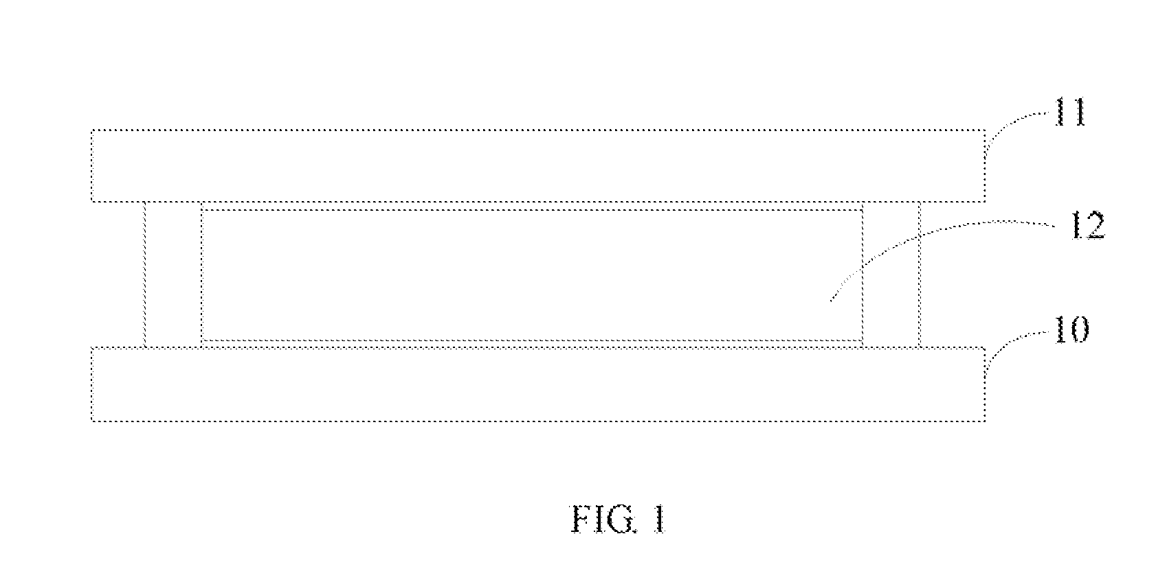
[0035]Referring to FIGS. 1-3, in a liquid crystal display panel of an embodiment of the present invention, the liquid crystal display panel comprises a first substrate 10, a second substrate 11, and a liquid crystal layer 12 sandwiched between the first substrate 10 and the second substrate 11; wherein the first substrate is an array substrate of the liquid crystal display panel and the second substrate is a color filter substrate of the liquid crystal display panel.

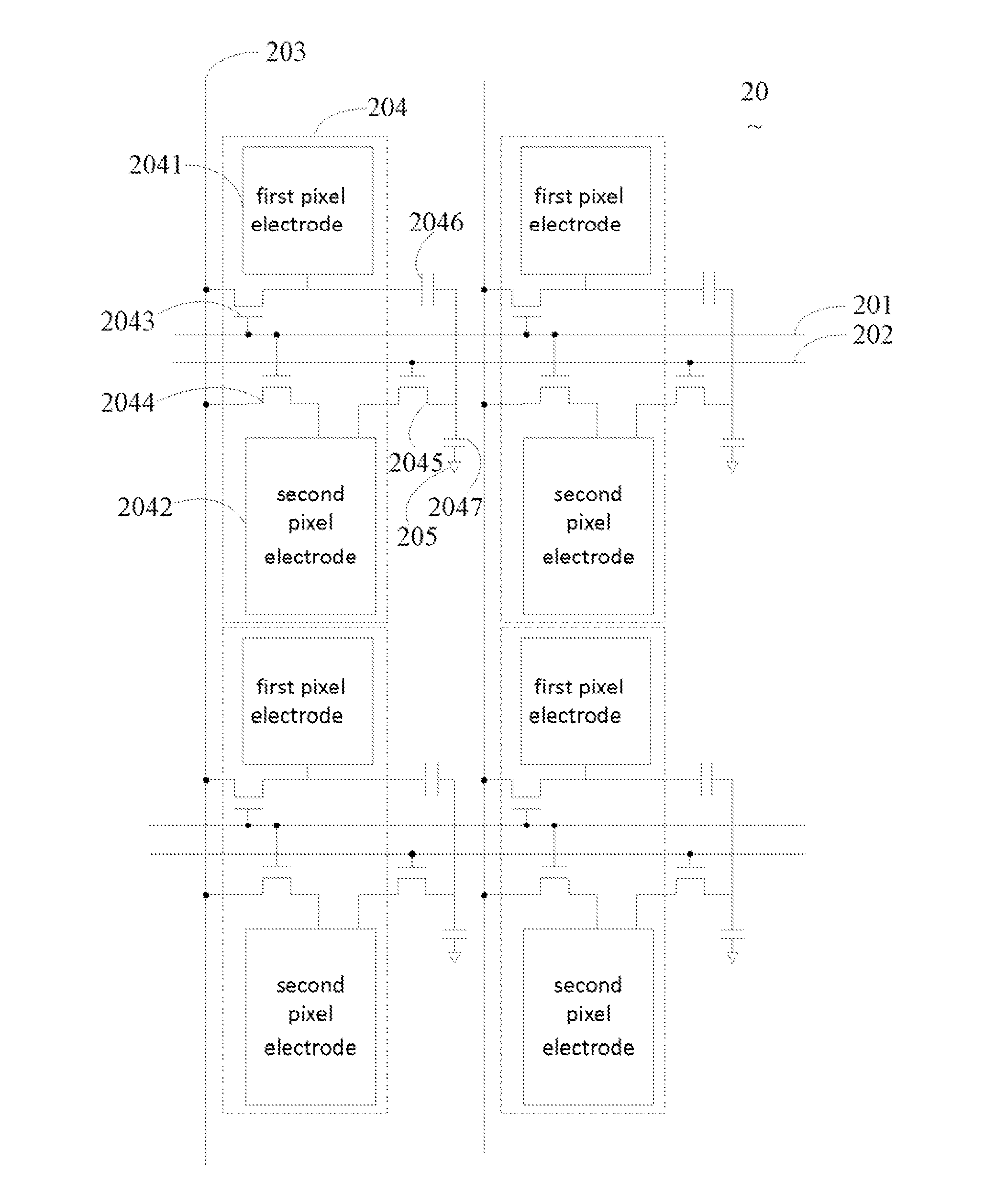
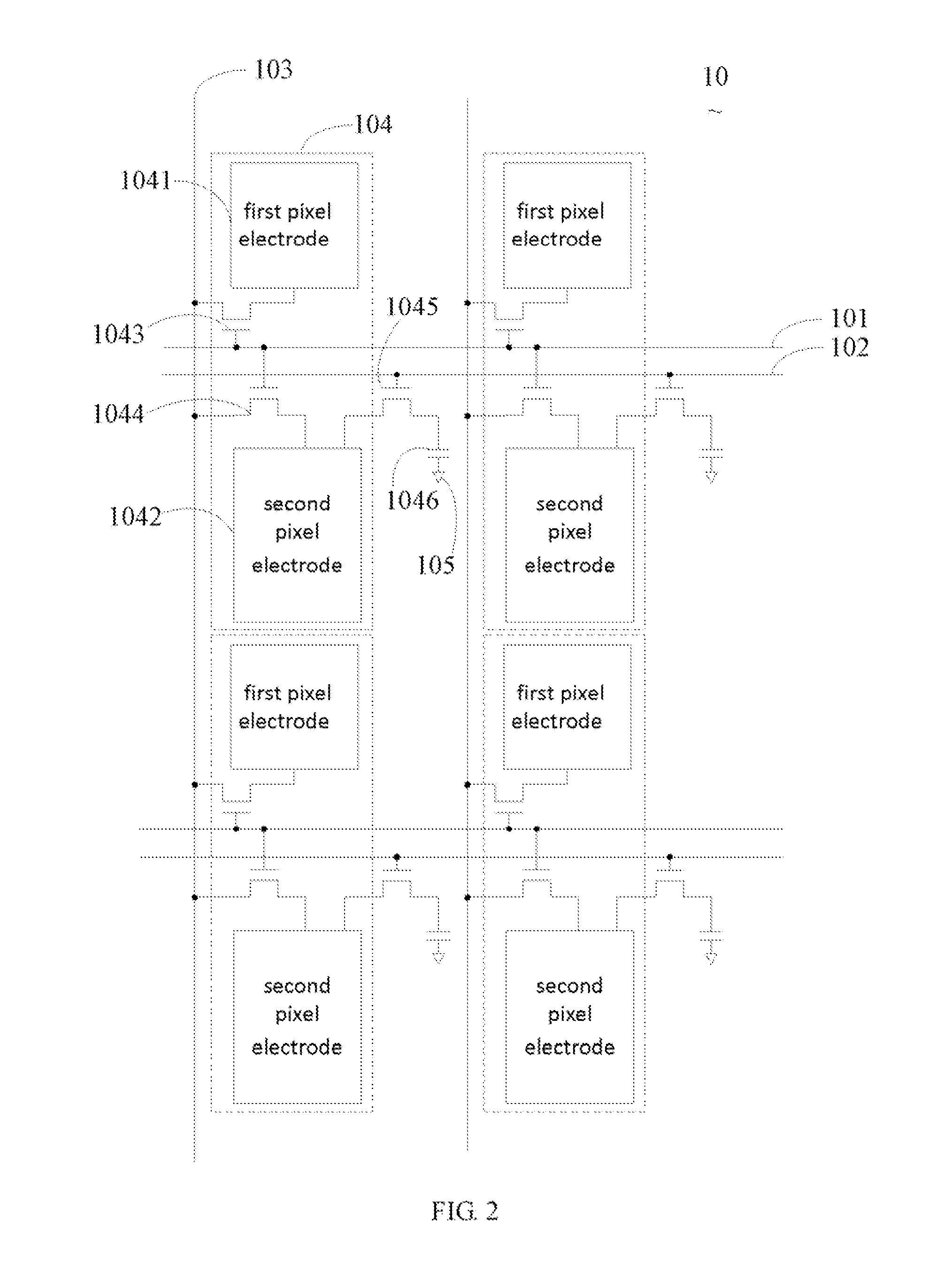
[0036]Further referring to FIG. 2, FIG. 2 shows a schematic view of the structure of the first substrate 10 of the present embodiment. The first substrate 10 comprises a plurality of charging scan lines 101, a plurality of discharging scan lines 102, a plurality of data lines 103 and, a plurality of pixel units 104, arranged in a matrix format. The plurality of charging scan lines 101 and the plurality of disc...


PUM


Abstract

The present invention provides a liquid crystal display panel and liquid crystal display device. In liquid crystal display panel, each pixel unit in the first substrate includes first pixel electrode and second pixel electrode. Charging scan line and data line drive first and second pixel electrodes to display through first switch and second switch. Third switch is connected to discharging scan line. Input terminal of third switch is connected to first or second pixel electrode; output terminal of third switch is connected to discharging circuit. Second substrate includes first common electrode and second common electrode. First common electrode corresponds to first pixel electrode and provides first common voltage. Second common electrode corresponds to second pixel electrode and provides second common voltage. As such, the present invention can further improve the low color shift at large viewing angle and effectively reduce the image retention problem.

Description

BACKGROUND OF THE INVENTION[0001]1. Field of the Invention[0002]The present invention relates to the field of liquid crystal displaying techniques, and in particular to a liquid crystal display panel and liquid crystal display device.[0003]2. The Related Arts[0004]The thin-film transistor liquid crystal display device (TFT-LCD) has gradually replaced the conventional CRT for the displaying market due to the advantages of small, thin, light-weight and flickering-free. However, in TFT-LCD often suffers the low color shift problem at large viewing angle. That is, when viewing at a large angle, the color distortion is more prominent, especially for the large-size LCD panel based on VA displaying technology. To solve the above problem, a common solution is to divide a pixel area on the array substrate into a main pixel area and a secondary pixel area so that the two areas display different Gamma curve. The composition of the Gamma curves of the two areas shows smaller viewing difference ...

Claims


Application Information

Patent Timeline
Patent Type & Authority Applications(United States)
IPC IPC(8): G09G3/36
CPCG09G3/3655G09G2320/0242G09G2300/08G09G2300/0426G09G2300/0447G09G2320/0276
Inventor DONG, CHENGCAI
Owner SHENZHEN CHINA STAR OPTOELECTRONICS TECH CO LTD
Why Eureka
Try Eureka