Substrate with spacer and liquid crystal cell containing the same
- Summary
- Abstract
- Description
- Claims
- Application Information
AI Technical Summary
Benefits of technology
Problems solved by technology
Method used
Image

Examples
first embodiment
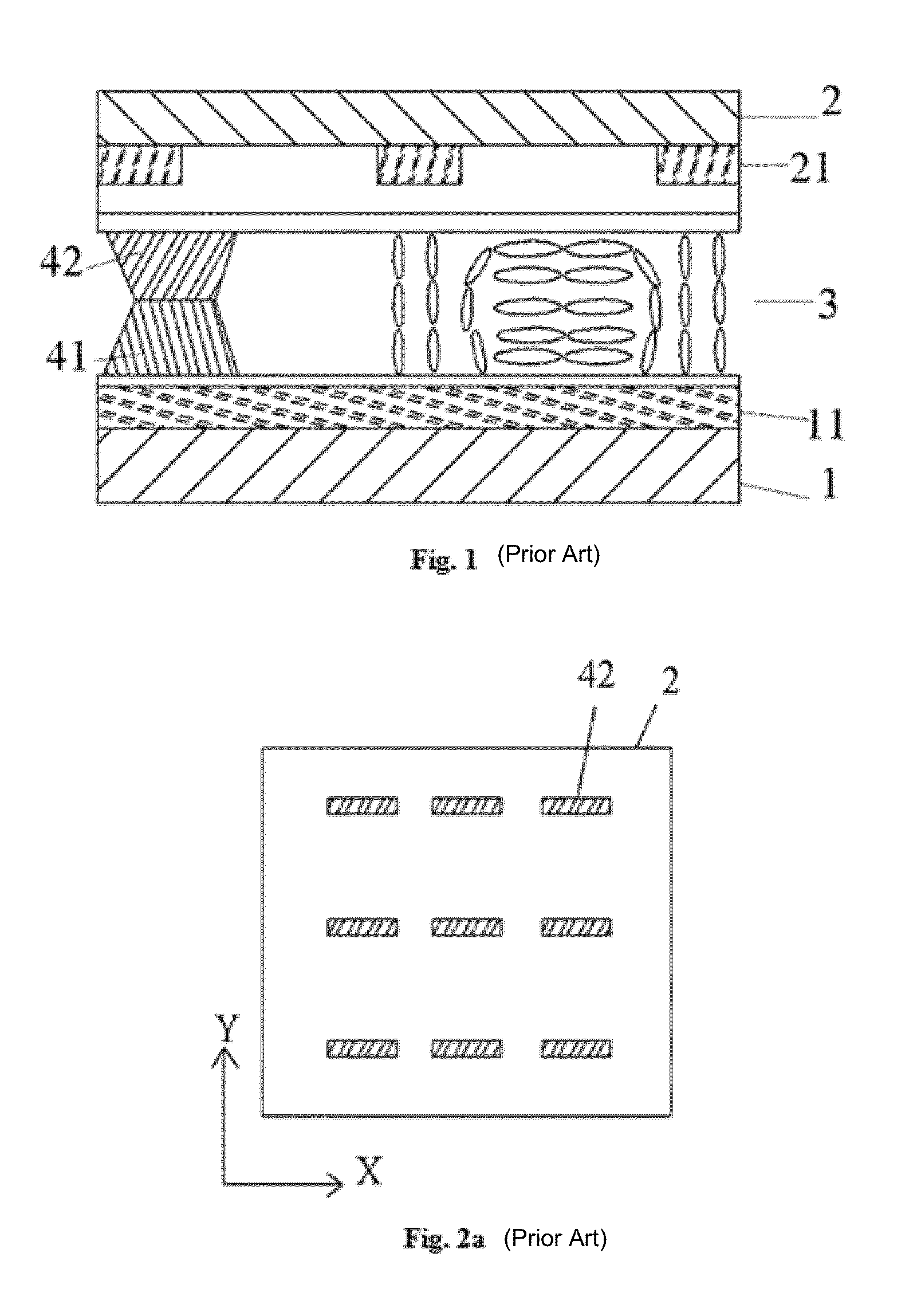
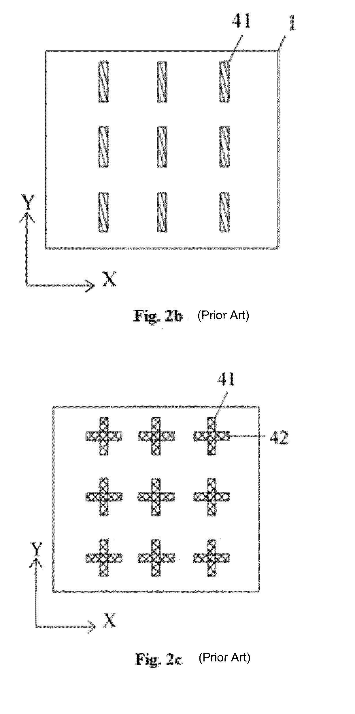
[0017]FIG. 3a and FIG. 3b are top views of a substrate structure according to a first embodiment of the disclosure. As shown in FIGS. 3a and 3b, a transparent substrate 5, such as a glass substrate, is prepared. Multiple spacers 51 are formed on the transparent substrate 5, which are arranged at a preset interval on one side of the transparent substrate 5. Generally, two spacers 51 may be provided, for example, in each square millimeter. Actually, the size of the spacer may be designed based on the size of the substrate and particular anti-pressure requirement. For a substrate with a great size (such as a substrate greater than 10 inches), due to its high anti-pressure requirement, the size of the spacer is designed to be great. The spacer 51 has a cross section taken in a direction parallel with the transparent substrate 5, and a size L of the cross section in a length direction is greater than a size W of the cross section in a width direction W, i.e., L>W. Specifically, in the em...
second embodiment
[0019]FIG. 4 is a cross sectional view of a liquid crystal cell according to a second embodiment of the disclosure. FIG. 5a and FIG. 5b are top views of the liquid crystal cell according to the second embodiment of the disclosure. As shown in FIG. 4, the liquid crystal cell includes a first substrate 5 and a second substrate 6 provided oppositely, and a liquid crystal layer 7 formed between the first substrate 5 and the second substrate 6. The first electrode 51 is a whole plane transparent electrode, and is formed on the side of the first substrate 5 that is close to the liquid crystal layer 7. The material of the first electrode 51 may be tin indium oxide. In conjunction with FIG. 5a, the second electrode 61 is a transparent electrode in a comb shape, which includes one end 611 and multiple comb tooth parts 612. The second electrode 61 is formed on a side of the second substrate 6 that is close to the liquid crystal layer 7. The first electrode 51 and the second electrode 61 are p...
third embodiment
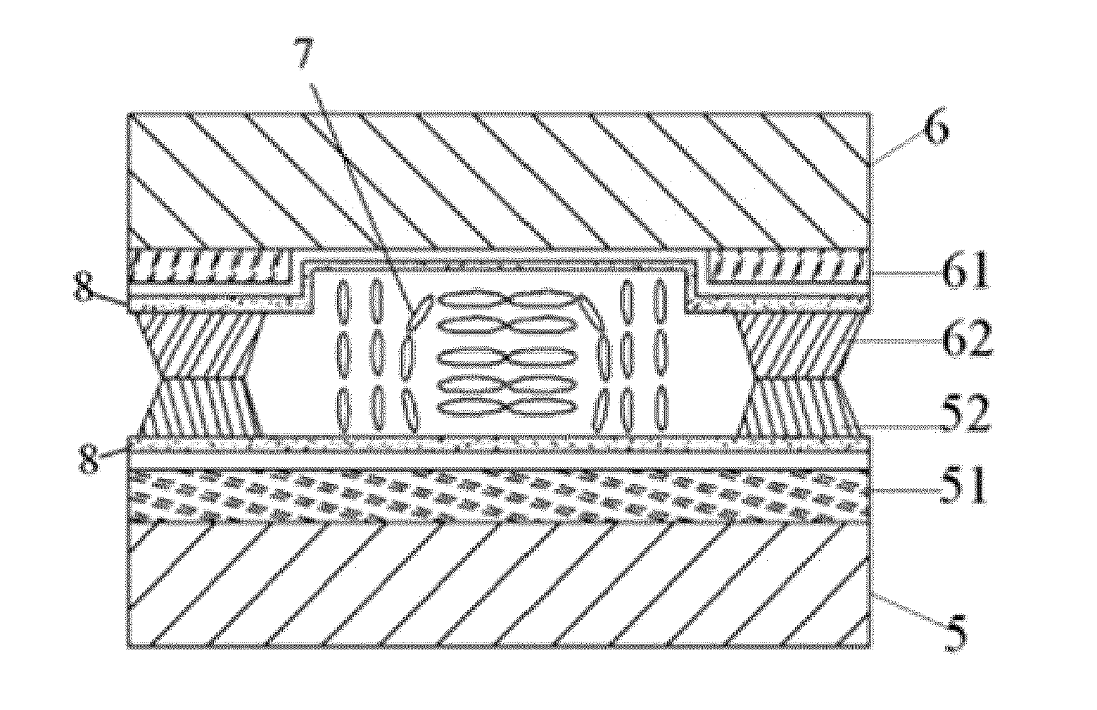
[0028]FIG. 6 is a cross sectional view of a liquid crystal cell according to a third embodiment of the disclosure. As shown in FIG. 6, the liquid crystal cell includes a first substrate 5 and a second substrate 6 provided oppositely, and a liquid crystal layer 7 formed between the first substrate 5 and the second substrate 6. The first substrate 5 is an array substrate, multiple thin film transistors 511 and pixel electrodes 512 are formed on a side of the first substrate 5 close to the liquid crystal layer 7. First spacers 52 are arranged at a preset interval on the first substrate 5. The second substrate 6 is a color filer substrate, and a black matrix 611 and a color resist 612 are formed on a side of the second substrate 6 close to the liquid crystal layer 7. Specifically, the black matrix 611 corresponds to the thin film transistor 511 on the first substrate 5 and serves to shelter, and second spacers 62 are provided on the region in which the black matrix 611 of the second sub...
PUM
 Abstract
Description
Claims
Application Information
 - R&D Engineer
- R&D Manager
- IP Professional
- Industry Leading Data Capabilities
- Powerful AI technology
- Patent DNA Extraction
Browse by: Latest US Patents, China's latest patents, Technical Efficacy Thesaurus, Application Domain, Technology Topic.
© 2024 PatSnap. All rights reserved.Legal|Privacy policy|Modern Slavery Act Transparency Statement|Sitemap