
Three-dimensional nonvolatile memory and related read method designed to reduce read disturbance

a nonvolatile memory and read method technology, applied in static storage, digital storage, instruments, etc., can solve the problems of different electrical parasitics of memory devices, and achieve the effect of substantially uniformizing the potential distribution of different cell strings and reducing read disturbances

Active Publication Date: 2015-01-08
SAMSUNG ELECTRONICS CO LTD
View PDF9 Cites 11 Cited by
  • Summary
  • Abstract
  • Description
  • Claims
  • Application Information

AI Technical Summary

Benefits of technology

The invention aims to reduce read disturbances by controlling the timing and levels of transistors in a memory device to ensure that boosted charges are evenly distributed. This results in a more uniform potential distribution in different cell strings.

Problems solved by technology

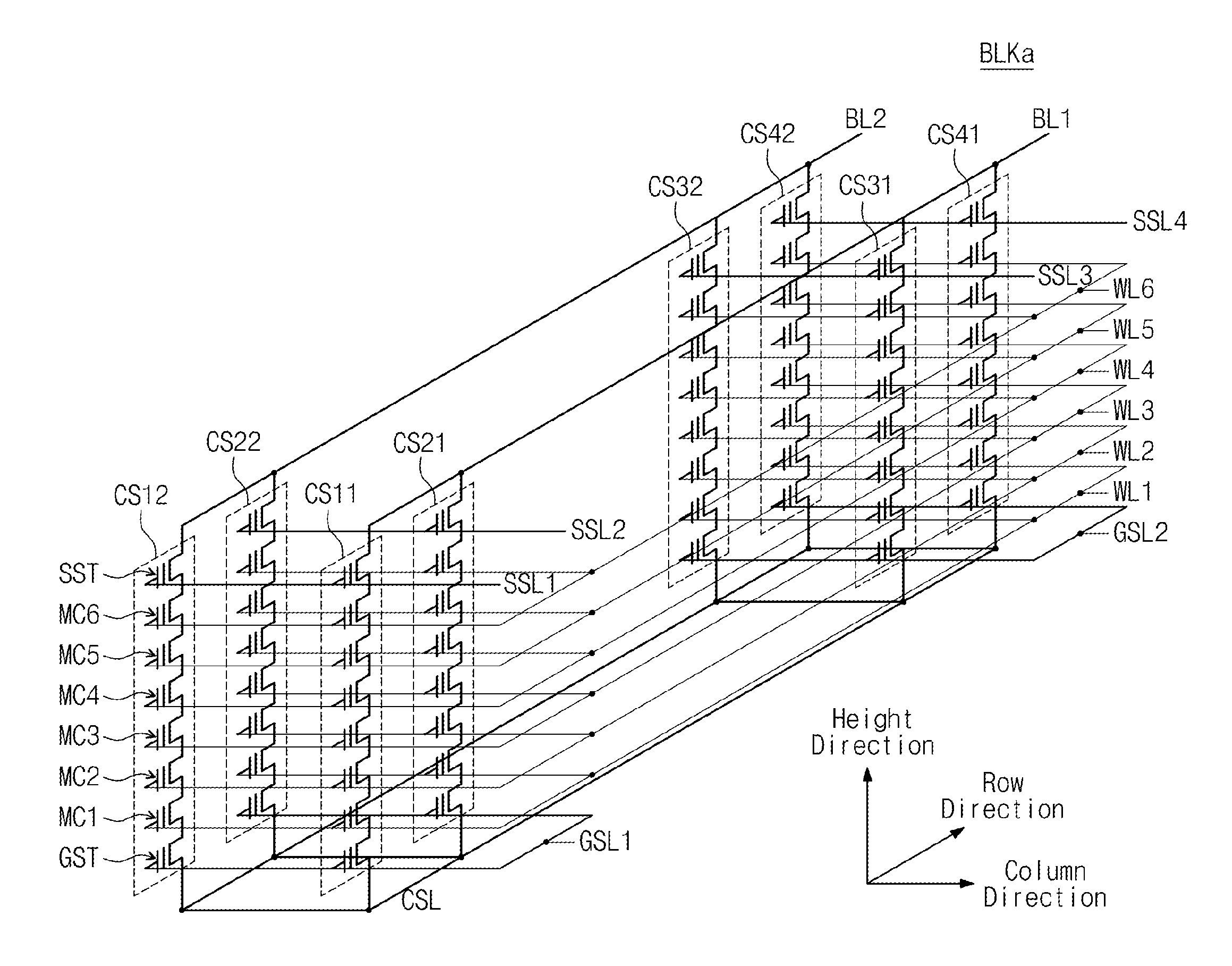
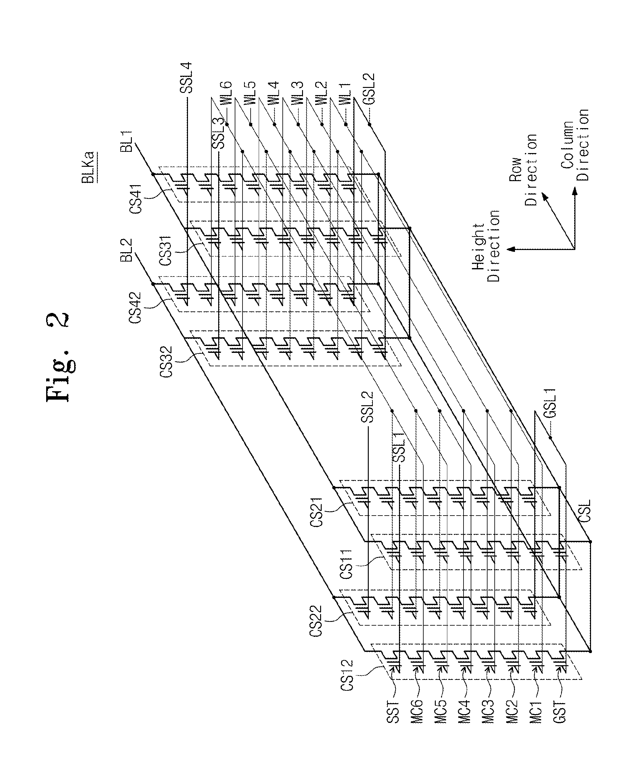
For example, due to their different structural characteristics, the 3D semiconductor memory devices may experience different electrical parasitics, which may require driving voltages to be provided with different levels and timing compared to 2D semiconductor memory devices.

Method used


Image

  • Three-dimensional nonvolatile memory and related read method designed to reduce read disturbance
  • Three-dimensional nonvolatile memory and related read method designed to reduce read disturbance
  • Three-dimensional nonvolatile memory and related read method designed to reduce read disturbance

Examples


Embodiment Construction

[0034]Embodiments of the inventive concept are described below with reference to the accompanying drawings. These embodiments are presented as teaching examples and should not be construed to limit the scope of the inventive concept.

[0035]In the description that follows, the terms “first”, “second”, “third”, etc., may be used to describe various features, but these features should not be limited by these terms. Rather, these terms are used merely to distinguish between different features. Thus, a first feature could be termed a second feature without departing from the teachings of the inventive concept.

[0036]Spatially relative terms, such as “beneath”, “below”, “lower”, “under”, “above”, “upper” and the like, may be used for ease of description to describe one feature's relationship to another feature(s) as illustrated in the figures. The spatially relative terms are intended to encompass different orientations of the device in use or operation in addition to the orientation depict...


PUM


Abstract

A nonvolatile memory device performs a read operation comprising first and second intervals. In the first interval the device applies a turn-on voltage to string selection lines and ground selection lines connected to the string selection transistors and the ground selection transistors, respectively. In the second interval, the device applies a turn-off voltage to unselected string selection lines and unselected ground selection lines while continuing to apply the turn-on voltage to a selected string selection line and a selected ground selection line. In both the first and second intervals, the device applies a first read voltage to a selected wordline connected to memory cells to be read by the read operation and applying a second read voltage to unselected wordlines among connected to memory cells not to be read by the read operation.

Description

CROSS-REFERENCE TO RELATED APPLICATIONS[0001]This application claims priority under 35 U.S.C. §119 to Korean Patent Application No. 10-2013-0022313 filed Feb. 28, 2013, the subject matter of which is hereby incorporated by reference.BACKGROUND OF THE INVENTION[0002]The inventive concept relates generally to semiconductor memory devices, and more particularly, to nonvolatile memory devices and related methods for performing read operations with reduced read disturbance.[0003]Semiconductor memory devices can be roughly divided into two categories according to whether they retain stored data when disconnected from power. These categories include volatile memory devices, which lose stored data when disconnected from power, and nonvolatile memory devices, which retain stored data when disconnected from power.[0004]Examples of volatile memory devices include static random access memory (SRAM) devices, dynamic random access memory (DRAM) devices, and synchronous DRAM (SDRAM) devices. Examp...

Claims


Application Information

Patent Timeline
Patent Type & Authority Applications(United States)
IPC IPC(8): G11C16/26G11C16/04
CPCG11C16/0483G11C16/26G11C16/3427G11C16/08G11C16/30G11C16/10G11C16/24
Inventor NAM, SANG-WANJUNG, WON-TAECK
Owner SAMSUNG ELECTRONICS CO LTD
Learn More