
Quad flat semiconductor device with additional contacts

a semiconductor device and flat package technology, applied in semiconductor devices, semiconductor/solid-state device details, electrical apparatus, etc., can solve the problems of increasing the complexity and functionality of electrical contacts, reducing the spacing between electrical contacts and the spacing between bond wires, and increasing the number of exposed electrical contacts

Active Publication Date: 2015-01-15
NXP USA INC
View PDF7 Cites 5 Cited by
  • Summary
  • Abstract
  • Description
  • Claims
  • Application Information

AI Technical Summary

Benefits of technology

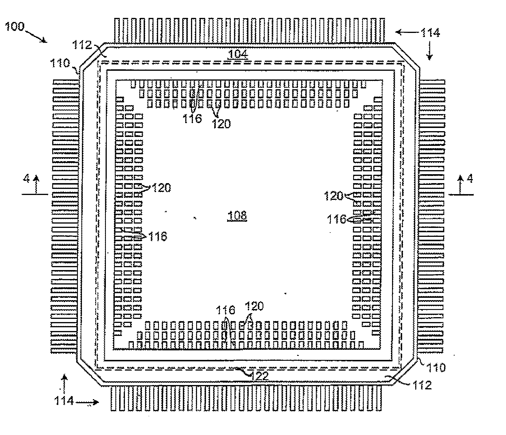
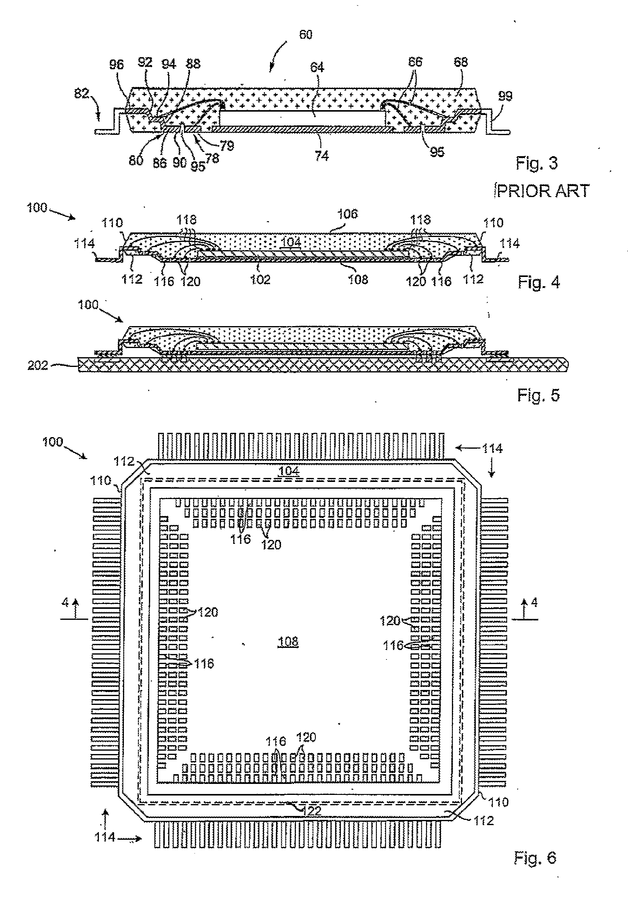
The present invention is directed to a QFP type semiconductor device with an additional row of external electrical contacts. The device has a molded package with a flag that is embedded in the mold compound. The exposed electrical contacts can be connected to the semiconductor die using wire bonding or lead frame techniques. The invention allows for more exposed electrical contacts and reduces the spacing between the bond wires. The method of assembling the device includes steps of mounting the semiconductor die on a lead frame, connecting the exposed electrical contacts to the die, and encapsulating the device. The invention provides a solution for increasing the number of exposed electrical contacts and reducing the size of semiconductor devices.

Problems solved by technology

Continued reduction in the size of semiconductor devices and increase in their complexity and functionality result in a need for an increase in the number of exposed electrical contacts and a reduction in the spacing between the electrical contacts and the spacing between the bond wires.

Method used


Image

  • Quad flat semiconductor device with additional contacts
  • Quad flat semiconductor device with additional contacts
  • Quad flat semiconductor device with additional contacts

Examples


Embodiment Construction

[0019]A conventional QFP device may include one or more rows of exposed electrical contacts on its bottom surface or face, in addition to leads projecting from its sides. The present invention makes available more bond zones for bottom face electrical contacts.

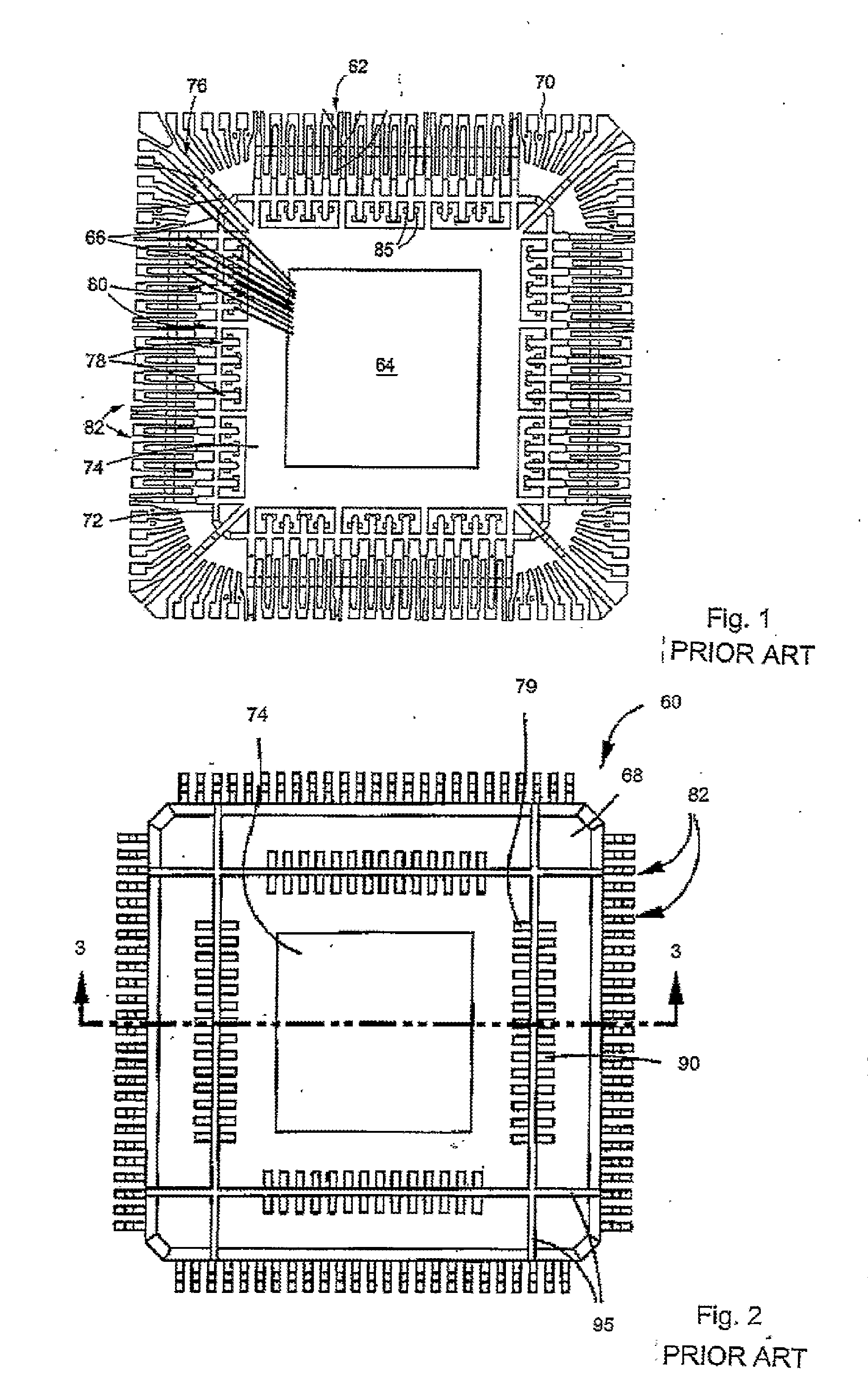
[0020]FIGS. 1-3 illustrate a conventional QFP device 60. The QFP device 60 comprises a lead frame 62, a semiconductor die 64 attached to the lead frame 62 and electrically connected thereto with bond wires 66, and a molding compound that encapsulates the die 64, bond wires 66 and partially encapsulates the lead frame 62, to form a package body 68 having top and bottom surfaces and sides or edge surfaces. The lead frame 62 includes a peripheral outer frame area 70. Located within the outer frame area 70 is a continuous, generally rectangular tie ring 72. The lead frame 62 also has a flag 74 upon which the die 64 is mounted. As shown in FIG. 1, the flag 74 is connected to the tie ring 72 with a tie bar 76.

[0021]The lead frame 62...


PUM


Abstract

A Quad Flat Package (QFP) semiconductor device has a multi-stepped lead frame for forming rows of external contacts. A semiconductor die is attached to a die pad of the lead frame and electrically connected to lead with bond wires. The die and bond wires are encapsulated with a mold compound and then multiple cuts are made to the lead frame to form the rows of external contacts.

Description

BACKGROUND OF THE INVENTION[0001]The present invention is directed to a quad flat package (QFP) type semiconductor device and, more particularly, to a QFP device have an additional row of external electrical contacts.[0002]Semiconductor device packaging fulfills basic functions such as providing electric connections and protecting the die against mechanical and environmental stresses. A surface mount semiconductor device has exposed electrical contacts that allow it to mounted on a support, such as a printed circuit board (PCB), for example, where its exposed electrical contacts provide for electrical communication with the PCB or with other circuitry or devices via the PCB. That is, the exposed electrical contacts of the device can be soldered directly to corresponding electrical contact pads on the support, providing mechanical attachment as well as electrical connections. Semiconductor devices are commonly packaged for surface mounting by encapsulating one or more semiconductor d...

Claims


Application Information

Patent Timeline
Patent Type & Authority Applications(United States)
IPC IPC(8): H01L23/495H01L23/00
CPCH01L24/83H01L23/49575H01L23/49541H01L23/49551H01L23/49555H01L21/4842H01L21/561H01L2224/4909H01L24/32H01L24/48H01L24/49H01L24/85H01L2224/32245H01L2224/48091H01L2224/49109H01L2224/73265H01L2224/83101H01L2224/8385H01L2924/181H01L2924/00014H01L2224/48247H01L2224/49433H01L2924/00012H01L2224/45099H01L2924/00
Inventor TIU, KONG BEEIBRAHIM, RUZAINI B.LO, WAI YEW
Owner NXP USA INC
Learn More